From pv magazine, December edition
Photovoltaics producers are bringing down electrical losses inside silicon solar cells by depositing nanoscopic layers of oxidized and polycrystalline silicon between their wafers and metal contacts. After racking up records in the laboratory, these so-called passivating contacts are finding their way into production lines. The European research centers and equipment manufacturers pioneering passivated contact technology expect it to deliver new momentum to EU solar technology suppliers.
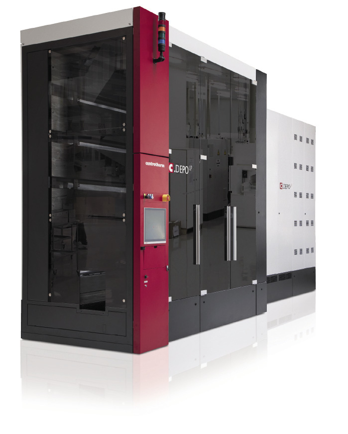
“Almost all big Chinese cell producers have bought one of our tools,” says Martijn Lenes, Business Director at Tempress, an equipment manufacturer based in Vaassen, the Netherlands. Over the past two years, Lenes has supplied a large number of customers with deposition lines for the new layers. “Some manufacturers just want to keep their options open,” he says. “But some are very serious about passivating contacts.” In recent weeks, Tempress has announced $11 million in deals with cell manufacturers, including one of the market leaders, Trina Solar, to ramp up the technology for mass production.
PV after PERC
“A lot of people see this as the next big step in photovoltaic technology,” says Professor Andres Cuevas from the Australian National University. He explains that the two thin layers reduce charge recombination at the interface between the wafer and metal contact of silicon solar cells. The first buffer layer is made of silicon oxide, typically less than two nanometers thick, and passivates dangling atomic bonds at the wafer surface. The second is a highly-doped layer of polycrystalline silicon that is poorly conductive for minority carriers, hence keeping them from reaching the surface where they are more likely to recombine.
“Introducing these buffer layers at the interface with metal contacts is the next logical step in photovoltaics manufacturing,” says Byungsul Min at the Institute for Solar Energy Research (ISFH) in Hamelin, Germany. He points out that technological advances between 2010 and 2012 focused on passivating solar cell emitters. Later, aluminum oxide increased passivation at cell surfaces. Now passivating contacts are tackling the next challenge on the list. “The interface between the metal contact and the silicon substrate has always been a very active recombination region,” he says. What has surprised the PV community is how rapidly advances in this field are bearing fruit.
New records
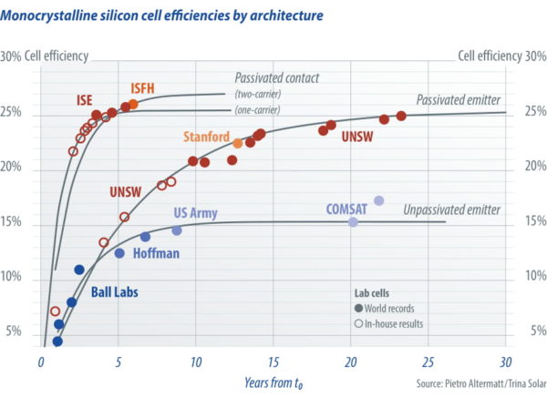
Earlier this year, the ISFH set a new record for p-type silicon solar cells, using passivating contacts to reach a conversion efficiency of 26.1%. Pietro Altermatt, Principal Scientist at Trina Solar, says that the achievement is all the more remarkable as the previous laboratory record built on 20 years of gradual advances in research and development. In contrast, passivating contacts have skyrocketed to the top of the class in barely five years. In parallel to records set in the laboratory, the technology has also broken ground on production lines.
According to Lenes, even the earliest deposition systems for passivating contacts commercialized by Tempress produced layers with extraordinary carrier lifetimes. “Our partners at ECN [the Energy Research Centre of the Netherlands] started measuring values of 8 milliseconds instead of 2 milliseconds on the first wafers,” he says. “They asked us what was in them. They just couldn’t believe it.”
This reduction in charge recombination rates has led to significant increases in the performance of solar cells. Loïc Tous at the imec research center on photovoltaics in Leuven, Belgium, says that passivating contacts typically increase open-circuit voltages of even high-range crystalline silicon cells from 680 mV to over 700 mV, boosting their energy conversion efficiency by close to half a percent. “An increase of 0.5% can mean a lot in the industry,” says Lenes.
In just a few years, passivating contacts have overtaken the energy conversion efficiency of low cost multicrystalline silicon photovoltaics, matched that of PERC technologies, and are even closing the gap with some of the priciest heterojunction silicon cells on the market. Strikingly, these milestones must be translated into mass production.
These prospects have drawn a vibrant research community to the field of passivating contacts. Names for the technology have multiplied as fast as record cells, with scientists at EU PVSEC, Europe’s premier solar conference for the research and manufacturing community, referring to them this year as POLO, Ox-Poly, PERPoly, carrier selective contacts, and deposited silicon junctions. The researchers at the Fraunhofer Institute, who arguably introduced passivation layers to the broader PV community in 2013, originally named them tunnel-oxide passivated contacts – or TOPCon – a name that has stuck with early adopters in industry. “When I talk with our Chinese customers, they call it TOPCon all the time,” says Lenes.
Popular content
Manufacturing challenge
In spite of excitement around passivating cell contacts, imec’s Tous warns that their commercial success hinges not only on efficiency, but on their complexity. Rival p-type PERC technology now mass produces solar cells with efficiencies also in the 22% range that are comparatively easy to make. “On the other hand, n-type PERT cells with passivating contacts typically require additional steps, additional equipment, silver contacts on both sides, and their n-type silicon wafer is also about 5% more expensive,” says Tous. These drawbacks incur costs that could break the business case for the technology and raise entry barriers for manufacturers.
“In general, the solar world is very conservative,” admits Lenes. “What cell producers don’t want to do is add new manufacturing steps.” That means adapting passivating contacts to established production processes. Tempress has optimized processes to deposit layers thickly enough to use screen printing techniques for their metallization (see box above). “If you talk with industrial producers they say that everything you do has to be compatible with screen printing,” says Lenes. He says that companies that have survived this long in the solar industry tend to be cautious by nature. While they are all testing the waters with passivating contacts, most will wait until a competitor makes money before fully adopting the technology themselves.
Trina Solar’s Altermatt explains the wisdom behind corporate patience. “Calculations by big Chinese manufacturers show that n-PERT cells with passivating contacts are not competitive,” he says, “mainly because their fabrication is so difficult.” Trina is delivering 1 GW of TOPCon n-PERT cells in March as part of China’s Top Runner program. Altermatt says that the very innovation of their production process inevitably raises challenges. “The chemical vapor deposition reactors we are using to make the passivating contacts get dusty with tiny silicon particles, their tubes sometimes crack and have to be replaced, that interrupts the production line,” he says. “There are all these aspects where I sometimes think: Why are we doing this?”
Altermatt is an active promoter of solar cell concepts beyond existing PERC technology, but he argues that passivating contacts offer more promise as incremental improvements than radical game changers. Rather than gamble the limited resources of cell manufacturers on comparatively uncharted n-type PERT cell structures, Altermatt suggests putting passivating contacts to work in structures more akin to established p-doped PERC.
He admits that this may result in lower efficiencies than TOPCon n-PERT, but it would also get more manufacturers on board. He says that pooling efforts could help develop the technology faster and ultimately in a more economical way. “PERC cells would offer a better platform to bring passivating contacts into the mainstream,” says Altermatt, “because they are already being mass fabricated.”
EU solar industry 2.0
Tempress remains neutral in the debate between n-type PERT and p-type PERC technology. Lenes points out that both solar cell structures would benefit from their deposition systems and that “big players have enough R&D capacity to explore this in both cell configurations.” He says that herd mentality within PV also has its benefits. “In some ways, it is desirable that companies do the same thing because it means that they are all developing along the same path,” he says. “That makes it easier for instance to optimize supply chains and build the critical mass to bring about new technologies.”
With leading photovoltaics manufacturers including Trina, LG, and Jolywood all launching passivating contacts in mass production, Lenes reports that the technology is picking up. Riding this momentum is vital for future equipment sales. “In the photovoltaics sector, you can never be sure that when you sell an R&D system [of the kind supplied in large numbers by Tempress], the client will also pick your brand for mass production. That is a risk you have to take,” says Lenes. “But our goal is that everybody grows accustomed to our specific process with our tools so that when they start ramping up, we’re their first choice.”
Commercial success could offer EU production equipment suppliers a second wind. “TOPCon rose to fame as a photovoltaic technology thanks to European research institutes. It is now entering commercialization thanks to European equipment,” says Lenes. Although cell manufacturing has largely collapsed in Europe, Lenes hopes that the region’s technological edge can open a more sustainable market for high-end innovative PV products and the equipment needed to fabricate them.
Benedict O’Donnell
This content is protected by copyright and may not be reused. If you want to cooperate with us and would like to reuse some of our content, please contact: editors@pv-magazine.com.

2 comments
By submitting this form you agree to pv magazine using your data for the purposes of publishing your comment.
Your personal data will only be disclosed or otherwise transmitted to third parties for the purposes of spam filtering or if this is necessary for technical maintenance of the website. Any other transfer to third parties will not take place unless this is justified on the basis of applicable data protection regulations or if pv magazine is legally obliged to do so.
You may revoke this consent at any time with effect for the future, in which case your personal data will be deleted immediately. Otherwise, your data will be deleted if pv magazine has processed your request or the purpose of data storage is fulfilled.
Further information on data privacy can be found in our Data Protection Policy.