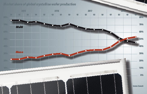
The eventual dominance of mono is almost universally accepted in the 2019 solar marketplace. But this was far from the case in late 2014 and 2015, when mono’s market share languished just north of 20%. Back then, there was considerable opposition to the forecast of mono’s rapid rise, and outright disbelief at the forecast that mono would overtake multi at some point in 2020. But the sheer pace of mono’s emergence has been astonishing, and illustrates how the right combination of performance, ease of manufacturing, and cost-effectiveness can drive rapid change in PV.
The holy trinity
Mono has consistently outperformed multi in terms of cell and module efficiency, but was hampered during the China growth years of 2008 to 2015 by high ingot growth costs and the lack of a mainstream cell architecture to take advantage of mono’s higher bulk quality. Together, these factors led to an uncompetitively high module cost per watt. But the maturing of three technologies in late 2014 and early 2015 – one at each of the ingot, wafer, and cell steps – led to a rapid reduction in mono module cost and a concurrent increase in efficiency, driving module cost per watt down to a market-leading level. These technologies are examined in more detail below.
High-productivity mono ingot growth
In the mid to late 2000s, a number of Chinese manufacturers installed Czochralski (CZ) pullers in expectation of imminent market growth, as multi approached what was widely expected to be its performance ceiling.
Yet far from stalling, multi remained on an impressive improvement path. Material and process cost reductions, combined with steady efficiency improvements, made it increasingly difficult for mono – with its relatively high ingot manufacturing costs – to keep up. Most of the directional solidification (DS) furnaces installed in the late 2000s wave of China PV capacity expansions were ‘Gen 4’ – that is, they grew multi ingots with 16 bricks (four bricks wide by four bricks deep), with a relatively large number of edge and corner bricks. While these DS furnaces offered much lower crystallization cost per kilogram (cost/kg), wafer quality was limited.
However, almost all of the DS furnaces purchased in that era were upgradable at low cost to Gen 7 (i.e. 49 bricks) and sometimes beyond, with relatively more of the higher quality center bricks and a consequent increase in average wafer efficiency. Other improvements, including seeded growth and rough-bottomed crucibles, contributed to ongoing efficiency gains that continued to surpass expectations. Eventually it became axiomatic that to bet against multi was a fool’s game. This thinking was what blinded many manufacturers to the resurgence of mono in 2015: They had been conditioned to believe multi would dominate in the foreseeable future. The eventual transition to mono, when it came, would be straight to n-type.
By 2015, the ‘easy wins’ on multi were becoming fewer. Upgrades beyond Gen 7 were expensive, and the rate of efficiency improvement was becoming harder to maintain, pushing multi developments increasingly into R&D and away from mainstream production. Meanwhile, changes were underway in mono ingot technology, including upgrading the standard CZ process to enable crucible recharge – known as recharge CZ. This was accompanied by other significant throughput enhancements, including substantial increases in the speed at which the grown ingot could be drawn from the melt, in part due to improved ingot cooling methods.
These mono ingot manufacturing improvements dramatically increased CZ productivity, reduced energy costs, and allowed more ingot to be pulled during the finite lifetime of expensive crucibles and graphite hot zones, reducing overall cost/kg. While these changes were not enough to bring mono ingot costs into parity with multi, they narrowed the gap significantly.
Diamond wire
Advances in sawing technology gave mono a huge advantage in 2015 and 2016. The replacement of the standard ‘slurry wire’ process with diamond wire reduced wafer costs in numerous ways. Aside from enabling a substantial reduction in kerf loss, it allowed manufacturers to dramatically increase saw productivity, reducing depreciation on existing equipment and enabling substantial capacity expansions at relatively low cost.
These diamond wire benefits were only available to mono, since the surface morphology of a diamond-sawn wafer was not amenable to the isotexture process used in multi wafering. Initially, savings from no longer having to use expensive silicon carbide/polyethylene glycol (SiC/PEG) slurries were offset by higher wire costs. But diamond wire prices began falling sharply, from more than $80/km in 2014 to less than $40/km in 2016, as a number of low cost, high quality Chinese manufacturers emerged and took share from foreign producers. Ongoing decreases in wire cost (close to $20/km today), reductions in wire diameter (with consequent kerf loss reductions and therefore more wafers per brick, which means more revenue per brick at a lower cost/wafer), and increases in cutting speed continued to reduce wafering costs, providing a crucial advantage to mono.
It wasn’t until 2017 that multi wafer texturing processes became widely available and in turn enabled diamond wire sawing of multi ingots. And this time lag was a crucial factor in opening the door to widespread mono adoption. By the end of 2017, the majority of multi wafering had switched to diamond wire, although mono continues to enjoy a slender advantage due to lower kerf loss and reduced wire usage.
PERC
Reduced wafer cost was just one piece of the puzzle. Equally critical was a mainstream high performance cell structure that took advantage of mono’s higher wafer quality to improve cell power.
Enter PERC and its rear-side passivation. While PERC technology worked on both multi and mono substrates (concerns over light-induced degradation, or LID, notwithstanding), the process conferred disproportionate efficiency benefits to mono, further expanding its performance advantage over multi at a stroke. A number of developments made high efficiency PERC cells possible at low cost in 2015: the emergence of cost effective PECVD-based solutions for depositing alumina layers on the rear of p-type cells, the development of appropriate aluminium pastes, and the deployment of low cost lasers for creation of ‘vias’ for rear contacts.
The efficiency gains achieved by mono PERC over its multi BSF and multi PERC rivals were advantageous in a critical way: They reduced the overall module cost per watt. Gains in cell efficiency translate into gains in module efficiency, bringing down the entire cost of the bill of materials (BOM) on a per watt basis.
By 2015, the era of huge BOM cost reductions was coming to an end. Costs for polysilicon, glass, EVA, backsheet, and other critical materials had, in the main, been reduced dramatically and the pace of absolute cost reduction was slowing. In order to achieve further cost/watt reductions it was becoming necessary to focus on driving up efficiency rather than simply driving down BOM unit costs. Against this background, the efficiency gains afforded by mono PERC were more than enough to compensate for additional ingot costs. Although mono requires higher grade polysilicon, the increased cost of this feedstock is outweighed by mono PERC’s efficiency gains.
Popular content
In a similar way, mono PERC also enables – in the near term at least – premium pricing. Since mono PERC’s increased power density translates into reduced LCOE at the system level, the system developer can pay a higher cost/watt for mono PERC modules but still improve the overall system economics. Premium pricing on a product that, on a fully integrated basis, is cheaper to make: What’s not to like?
Integration
Critically, each of these three technologies could be integrated into existing manufacturing processes with comparative ease. Feeders were widely used to reload the CZ crucible between ingot runs, with no changes to the puller itself. Diamond wire required comparatively minor modifications to existing saws, plus a change of one consumable (the wire) and the elimination of two others (SiC and PEG). And PERC delivered a huge increase in cell efficiency that justified the investment in relatively modest equipment additions.
Next, mono ingot and wafer manufacturing had to scale. A small mono manufacturer, Longi, had been around since 2009, improving its processes and growing modestly to about 3 GW of capacity in 2014. But in 2015 it shifted gears and began to scale rapidly, shouldering the burden, alongside Tianjin Zhonghuan Semiconductor, of growing mono capacity.
With widespread availability of low-cost mono wafers by 2016, the move to mono PERC was now relatively simple for cell manufacturers: Upgrade the cell lines to PERC, modify the cell texture process, and purchase cheap, high performance mono wafers.
The Chinese government’s Top Runner program also helped to advance mono by mandating the use of higher efficiency modules in government projects. However, we see this as a case of accelerated inevitability: Mono PERC’s lower cost and higher performance were destined to win, regardless of policy support.
The future ain’t what it used to be
New technologies must improve performance, or at worst, deliver the same performance at reduced cost. Gone are the days when manufacturers could expect to achieve huge cost reductions from materials alone. But improved performance is not enough – new technologies must not increase cost/watt. An exotic IBC structure might deliver high efficiency, but unless it reduces LCOE, what’s the point? And a new technology that requires radical changes to existing processes, or requires manufacturers to write down expensive investments in existing equipment, will always be a tough sell.
Exawatt’s view is that the ‘next big thing’ will satisfy the following rule: It must deliver a significant increase in performance at acceptable cost, with minimal integration challenges.
Applying this rationale to some technologies that are in the mix right now forms the core of Exawatt’s current research work. At a very high level, here are some examples of how the above rule might be applied.
Heterojunction (HJT)
HJT cell technology is relatively mature, delivers excellent module performance at a potentially competitive cost, but is a challenging cell process to integrate, requiring a number of steps that are not part of mainstream cell lines. It may prove to be viable, but for greenfield manufacturing only.
Tunnel Oxide Passivated Contacts (TOPCon) cells may neatly solve HJT’s integration issue. However, the technology is less mature than HJT and so mass production efficiencies and costs are as yet unknown.
Kerfless wafer
At the ingot/wafer level, the kerfless wafer technologies that appear closest to large-scale production promise reduced costs in theory (i.e. at large scale and high yield), but capital cost and productivity are unclear. In addition, wafer quality remains a concern. Any technology that produces wafers that are not capable of competing on performance with mono PERC may just exchange a silicon cost saving for a cost/watt increase on the rest of the BOM (due to lower module efficiency), and may even increase LCOE. Kerfless wafers made a lot of sense when polysilicon pricing was in the hundreds of dollars per kg, but the investment case has eroded ever since.
In the longer term, high efficiency perovskite/silicon tandem cells hold promise, but it’s far from clear that the key challenge of combining efficiency with long-term stability in the same cell construction has been overcome. If this can be achieved then improved performance should be a given, although impacts on costs and ease of integration are as yet unknown. ![]()
The views and opinions expressed in this article are the author’s own, and do not necessarily reflect those held by pv magazine.
This content is protected by copyright and may not be reused. If you want to cooperate with us and would like to reuse some of our content, please contact: editors@pv-magazine.com.

3 comments
By submitting this form you agree to pv magazine using your data for the purposes of publishing your comment.
Your personal data will only be disclosed or otherwise transmitted to third parties for the purposes of spam filtering or if this is necessary for technical maintenance of the website. Any other transfer to third parties will not take place unless this is justified on the basis of applicable data protection regulations or if pv magazine is legally obliged to do so.
You may revoke this consent at any time with effect for the future, in which case your personal data will be deleted immediately. Otherwise, your data will be deleted if pv magazine has processed your request or the purpose of data storage is fulfilled.
Further information on data privacy can be found in our Data Protection Policy.