Researchers from the University of Rajshahi in Bangladesh and the Saitama University in Japan have demonstrated a cadmium telluride (CdTe)-based dual-heterojunction solar cell that incorporate cadmium selenide (CdSe) and antimony selenide (Sb2Se3).
“The proposed structure was designed and simulated,” research co-author Jaker Hossain told pv magazine. “It is not tested in real PV modules yet, but we are in the midst of making real cells.” He also explained that CdSe and CdTe were already manufactured through a spin coating method and that the research group is now focusing on the solution process for CdSe and Sb2Se3 back surface field (BSF) layers. “And then, we will prepare the practical cell,” he added.
In the paper “Design of a highly efficient CdTe-based dual-heterojunction solar cell with 44% predicted efficiency”, published in Solar Energy, the scientists explained that CdSe is an n-type II-VI semiconductor with a direct bandgap of 1.7 eV that is largely utilized in light-emitting diodes, solar cells and photoelectrochemical cells. Sb2Se3 is described as a p-type inorganic semiconductor with an orthorhombic crystal structure and a direct bandgap in the range of 1.2 to 1.9 eV.
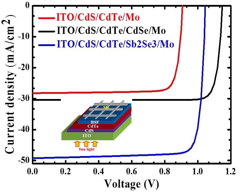
The group investigated, in particular, the impact of the addition of a CdSe BSF layer on the heterojunction cell performance, depending on the layer's different thickness and charge carrier density. For example, they ascertained that the cell open-circuit voltage increased from 0.89 to 1.1 V when the BSF layer thickness raised from 0 to 50 nm and the short-circuit current from 28.5 to 31.5 mA/cm2 when the thickness climbed from 0 to 200 nm. An overall increase of cell efficiency was observed for the CdSe thickness of over 50 nm together with a smaller decrease of the short-circuit current.
For the simulated cell, the research team reported the highest efficiency of 32.6% with a thickness of 100 nm, which also provided an open-circuit voltage of 1.15 V, a short-circuit current of 32.48 mA/cm2 and a fill factor of 88.76%.
By increasing the carrier concentration in the CdSe BSF layer and maintaining a thickness of 50 nm, the scientists were able to increase the conversion efficiency of the simulated cell to 44.14%. For this device, the short-circuit current was 49.23 mA/cm2, the open-circuit voltage 1.05 V and the fill factor 85.71%.
Popular content
“This investigation on deferent interface defect density suggests that the interface defect density has a massive impact on the performance of the CdTe-based dual heterojunction solar cells,” the paper notes. “The interfacial defects are induced by the structural defects of the two respective materials and diffusion of metal cations through the absorber layer during cell fabrication are the key sources of the interface defect.”
The impact of interface defect, however, can be minimized by the utilization of efficient deposition techniques and a highly attentive concentration of Sb2Se3 during fabrication of the cell, according to the researchers.
This content is protected by copyright and may not be reused. If you want to cooperate with us and would like to reuse some of our content, please contact: editors@pv-magazine.com.


By submitting this form you agree to pv magazine using your data for the purposes of publishing your comment.
Your personal data will only be disclosed or otherwise transmitted to third parties for the purposes of spam filtering or if this is necessary for technical maintenance of the website. Any other transfer to third parties will not take place unless this is justified on the basis of applicable data protection regulations or if pv magazine is legally obliged to do so.
You may revoke this consent at any time with effect for the future, in which case your personal data will be deleted immediately. Otherwise, your data will be deleted if pv magazine has processed your request or the purpose of data storage is fulfilled.
Further information on data privacy can be found in our Data Protection Policy.