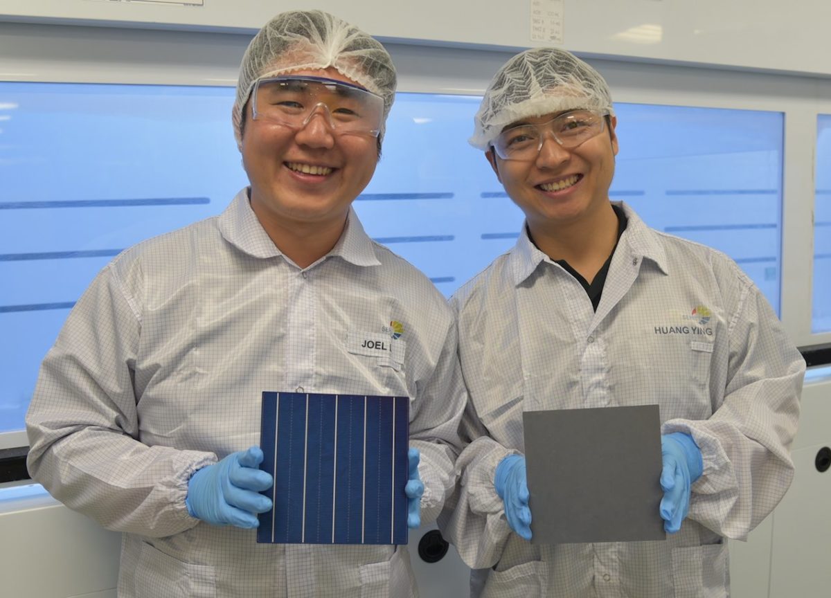
A team of scientists at SERIS has announced the development of a new process for the texturing of diamond wire cut multicrystalline silicon (multi-cSi) wafers.
The wet chemical technique etches the wafer surface with nano-scale features, which increases the chance of light bouncing off the surface multiple times and being absorbed by the wafer material.
According to SERIS, the technique uses proprietary chemicals and is low-cost, scalable and can be easily integrated into cell production lines.
The advent of diamond wire sawing several years ago brought major cost reductions to PV manufacturing, but owing to the texturing issue, the technology was initially limited to monocrystalline silicon wafer.
Several solutions to this are already commercially available, including ‘black silicon’ techniques of reactive ion etching, metal catalyzed chemical etching, and the DW Pretex Process developed by German company Schmid.
Despite this, SERIS is confident that its new process offers further benefits to manufacturers, particularly in comparison to the black silicon processes.
Popular content
“The two techniques that are commonly used to create a nanoscale texture on DWS mc-Si wafer surfaces are reactive ion etching (RIE) and metal-catalysed chemical etching (MCCE). The production costs of these two techniques are much higher than those of conventional acid-based texturing, and MCCE involves the use of metallic particles which runs the risk of introducing contaminants to production lines,” says Huang Ying, lead inventor of the DWS wafer texturing technology.
“Our technology is simpler, cheaper, metal-free and can achieve cell efficiencies of more than 20%. For these reasons, I strongly believe that our technology can become a mainstream texturing technology used by mc-Si solar cell manufacturers.”
SERIS says its process has already been recognized by several tier-1 manufacturers, and that it plans to work closely with them to see the process scaled up to large production lines.
“As the PV industry experiences a major shift from slurry-cut to DWS mc-Si wafers this year, we believe that this novel technology developed by SERIS will become a mainstream texturing technology for DWS mc-Si wafers,” says SERIS CEO, Armin Aberle.
This content is protected by copyright and may not be reused. If you want to cooperate with us and would like to reuse some of our content, please contact: editors@pv-magazine.com.


Is it PERC process included for the efficiency which more than 20% as mentioned above? By the way, how about the efficiency achieved in the traditional process which without PERC process?