Gallium-arsenide (GaAs), and other cell materials from the III-V group, have long been an area of interest for researchers working in solar PV thanks to their potential for very high efficiency. The cost of the materials, however, has kept these materials limited to niche applications such as drones and space travel.
Making the devices thinner, minimizing use of the valuable materials, is one well-explored approach to bring down manufacturing cost. And for the niche applications where GaAs is already viable, weight reduction achieved by making a device thinner is a valuable prospect, and thinner devices also show improved resistance to the higher radiation levels outside of Earth’s atmosphere.
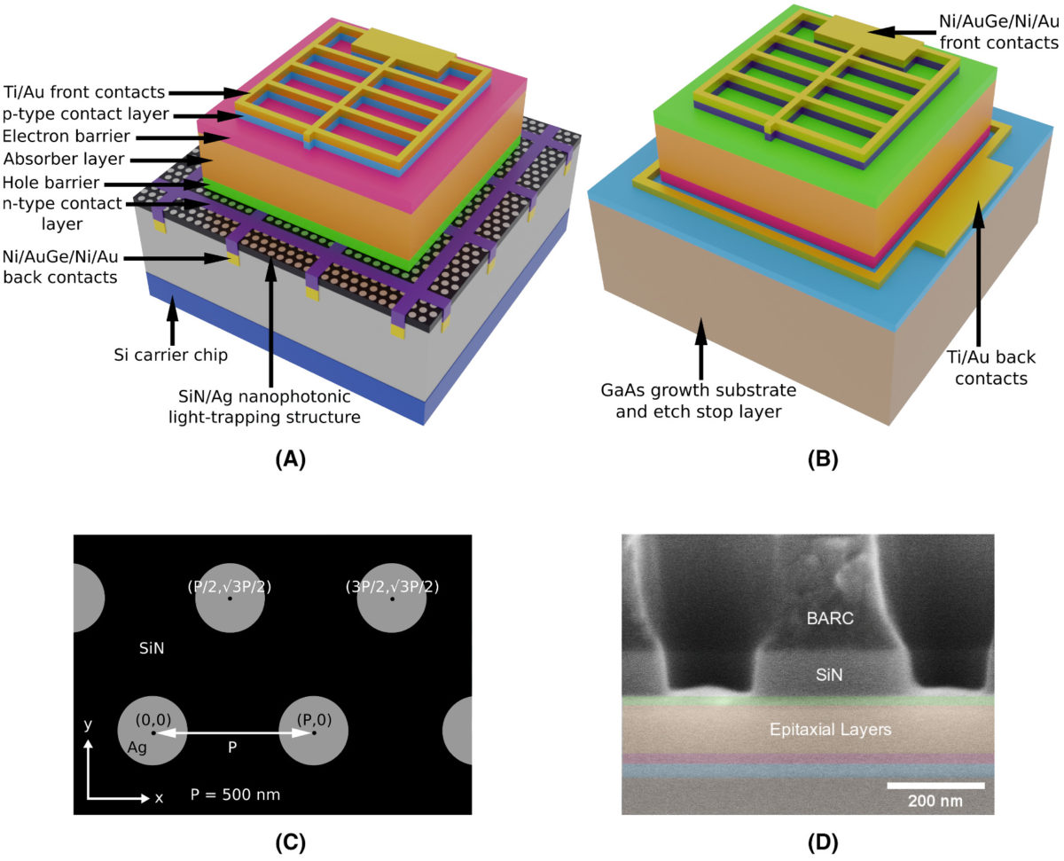
Maintaining high efficiencies, however, becomes a challenge as thickness is reduced, because there is less material available to absorb the light. Adding light management structures, that can trap photons for longer and increase their chance of being absorbed and converted to electricity. This was the approach taken by scientists at Cambridge University in the UK, who aim to overcome the efficiency challenges with ultrathin devices, allowing them to take advantage of their lower weight and intrinsic radiation resistance.
“Intrinsic radiation tolerance that has previously been demonstrated on this length scale is sufficient to enable new mission types in hostile environments as well as lightweight flexible form factors by reducing or eliminating the need for protective coverglass,” the group stated. “However, the ultra-thin absorbers are highly transmissive and require integrated light management to increase current.”
Popular content
The group fabricated GaAs cells just with an active layer just 80 nanometers (nm) thick, adding up to 120 nm when window and back surface field layers are added. Using a patterning technique known as displacement talbot lithography (DTL), the group integrated light management architectures onto the cells and compared their performance to cells to others that integrated a planar silver mirror to reflect light back to the cell. “[DTL] is inherently suited to wafer-scale, high throughput fabrication and therefore a feasible approach for manufacturing large area photovoltaic devices with integrated light management,” they explained.
The devices are described in the paper Ultra-thin GaAs solar cells with nanophotonic metal-dielectric diffraction gratings fabricated with displacement Talbot lithography, published in Progress in Photovoltaics. The group was able to demonstrate 9.08% efficiency – a 68% improvement compared to a device that used on-wafer processing.
Using simulations, the group was further able to demonstrate that the addition of an anti-reflective coating, and further innovations to reduce frontside grid surface shading, could quickly boost this efficiency to 16%. They note that while this type of device is unlikely to be useful for mainstream PV applications, they hope to open new possibilities for power generation in space, and other potential applications. “These results show that future embodiments of ultra-thin devices are unlikely to complete with current industry standard multijunction photovoltaics on efficiency alone,” they conclude. “However, the potential efficiency gains of nanophotonic integration demonstrated here, alongside low mass and inherent radiation tolerance, might enable new mission profiles and launch cost reductions, making ultra-thin devices a compelling platform for development.”
This content is protected by copyright and may not be reused. If you want to cooperate with us and would like to reuse some of our content, please contact: editors@pv-magazine.com.


By submitting this form you agree to pv magazine using your data for the purposes of publishing your comment.
Your personal data will only be disclosed or otherwise transmitted to third parties for the purposes of spam filtering or if this is necessary for technical maintenance of the website. Any other transfer to third parties will not take place unless this is justified on the basis of applicable data protection regulations or if pv magazine is legally obliged to do so.
You may revoke this consent at any time with effect for the future, in which case your personal data will be deleted immediately. Otherwise, your data will be deleted if pv magazine has processed your request or the purpose of data storage is fulfilled.
Further information on data privacy can be found in our Data Protection Policy.