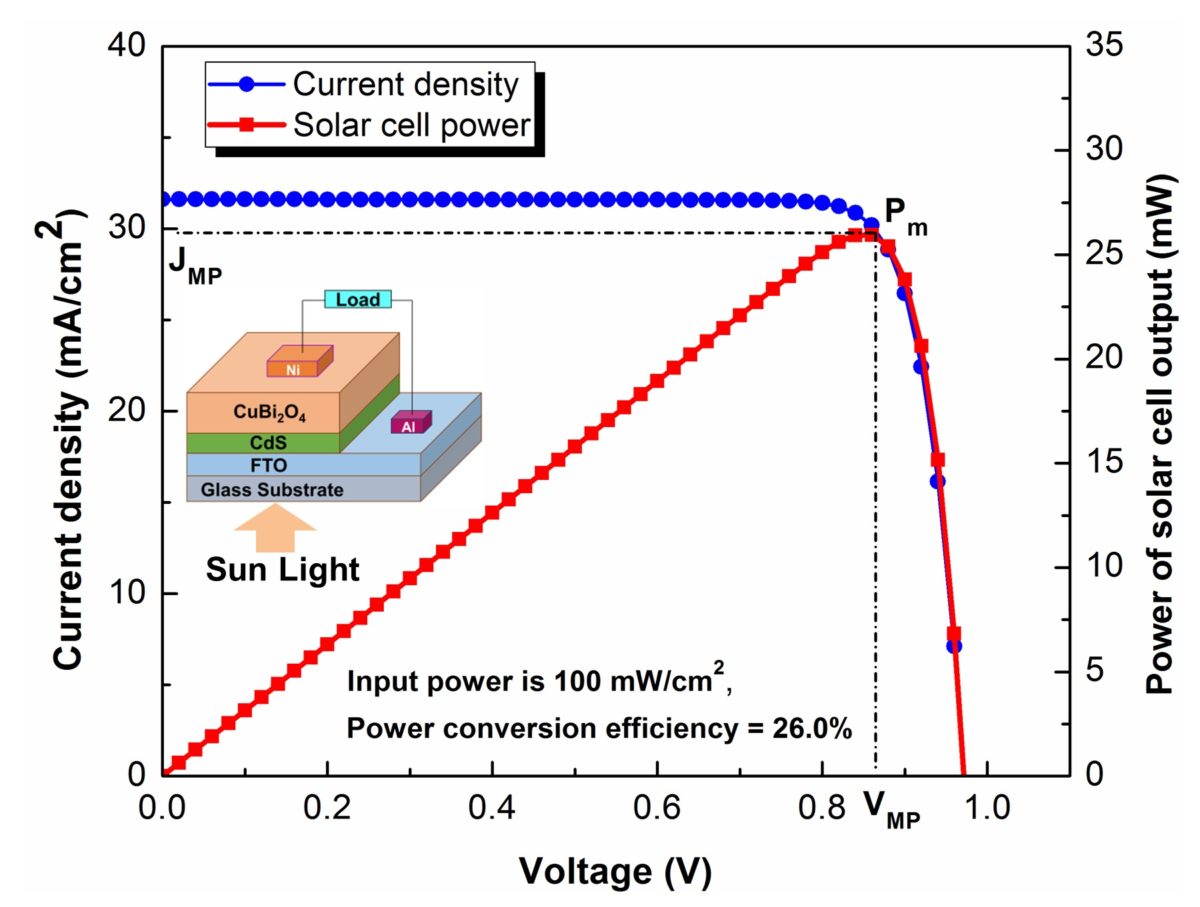
Researchers at the Pabna University of Science and Technology, in Bangladesh, have simulated a thin-film solar cell based on copper bismuth oxide (CuBi2O4), which is a p-type semiconductor that has been recently identified as a photocathode with a two-dimensional porous heterojunction structure.
“CuBi2O4 is an abundant, inexpensive, and harmless p-type metal oxide semiconductor,” research co-author, Sheikh Rashel Al Ahmed, told pv magazine. “Highly scalable techniques such as magnetron sputtering and spin coating can be used to fabricate high-density p-type CuBi2O4 thin films at a high deposition rate and low cost.”
CuBi2O4 has a high optical absorption coefficient and has, also, the advantage of a having narrow energy bandgap, from 1.4 to 1.8 eV, which the researchers recall, is near the optimum value for solar cell applications.
The proposed cell, described in the study Simulating the performance of a highly efficient CuBi2O4-based thin-film solar cell, published in SN Applied Sciences, has a heterojunction architecture in which the CuBi2O4 material is used as an absorber and n-type cadmium sulfide (CdS) is utilized as a buffer layer. The device also incorporates an aluminum (Al) film, a fluorine-doped tin oxide (SnO2:F or FTO) as a window layer, and a nickel (Ni) layer.
The cell configuration is the following: Al/SnO2:F(FTO)/CdS/CuBi2O4/Ni. The CuBi2O4, CdS, and FTO layers had a thickness of 2.0μm, 0.06μm, and 0.05μm, respectively. “The thickness of the proposed CuBi2O4 solar cell is thin enough, as compared to the similar photovoltaic devices employing other toxic absorber materials, and thus reduces the overall costs of the cell fabrication,” Al Ahmed explained.
Popular content
In the simulation, the cell was illuminated under AM1.5G solar spectrum with 100 mW/cm2 incident power density. “The efficiency of 26.0% with open-circuit voltage of 0.97 V, short-circuit current density of 31.61 mA/cm2, and fill factor of 84.58% is achieved for the proposed solar cell at the optimum 2.0μm-thick CuBi2O4 absorber layer,” the paper notes.
“The proposed cell design is not tested in a real device but, in the near future, practical production details will come in,” Al Ahmed further explained. “To achieve pertinent insight into the desirable aspect of such devices in practical applications, the numerical investigation of the structural performance, and understanding the physics of solar cells, could be a convenient approach.”
According to him, the numerical modeling techniques could be used to forecast the variations in material properties and furnish important suggestions to change designs and parameters. “Prior to the solar cell fabrication, the device simulations for thin-film heterojunction solar cells are necessary to understand the operation mechanism,” he concluded.
This content is protected by copyright and may not be reused. If you want to cooperate with us and would like to reuse some of our content, please contact: editors@pv-magazine.com.


New and cost effective solar technology is urgently needed . I think batteries are still the more expensive component of the system . Sec