Scientists propose solar cell taxonomy based on absorber integration

Researchers from the University of León in Spain have proposed a new solar cell technology classification intended to bring clarity to the growing diversity of photovoltaic technologies and overcome the limitations of the conventional generation-based taxonomy.
Whereas the conventional taxonomy classifies photovoltaic technologies primarily according to successive technological “generations,” the proposed taxonomy replaces this chronological hierarchy with a structure- and physics-based classification defined by how the absorber is integrated into the device and by the dominant mechanisms governing photoconversion and charge transport.
“Instead of asking which ‘generation’ a photovoltaic technology belongs to, we ask a simpler physical question: how is the light-absorbing material actually integrated into the device? That shift reveals structural relationships that a chronological classification can easily obscure,” corresponding author Ana-María Diez-Suárez told pv magazine.
“This classification grew out of a very practical need in my PhD research: how can we compare very different photovoltaic technologies without forcing them into generations that no longer explain clearly how the devices are built or why their limitations differ? Starting from absorber integration gives us a common language linking architecture, operation, and degradation,” first author Marta Martínez-Benavides added.
“One thing this framework makes clearer is why technologies with apparently similar performance targets can face very different manufacturing and scalability challenges. How the absorber is formed, supported, and integrated into the device is a fundamental constraint — one that the conventional generational scheme does not make explicit,” said co-author Jorge-Juan Blanes-Peiró.
Presented in the paper “Rethinking the classification of photovoltaic technologies through absorber integration,” published in Solar Energy, the new approach organizes photovoltaic technologies into four groups according to absorber integration and the dominant physical mechanisms governing device operation. The analysis covers architecture, materials, fabrication, performance, stability, and technological limitations, enabling direct comparisons among otherwise very different photovoltaic platforms.
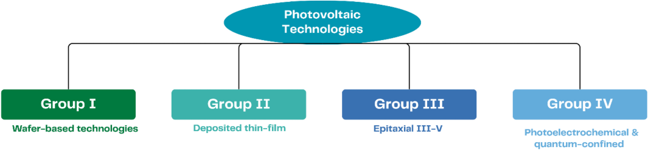
The first group comprises wafer-based technologies in which the absorber itself forms the active structural substrate, including aluminum back surface field (Al-BSF), passivated emitter and rear cell (PERC), tunnel oxide passivated contact (TOPCon), silicon heterojunction (HJT), and back-contact architectures.
Their technological evolution is characterized primarily by the progressive reduction of bulk and surface recombination through improved passivation and carrier-selective contacts. The transition from Al-BSF to PERC and subsequently to TOPCon illustrates the shift from direct metal contacts toward increasingly sophisticated passivated interfaces. HJT extends this strategy through amorphous/crystalline silicon heterojunctions, while interdigitated back-contact (IBC) architectures reduce optical losses by relocating contacts to the rear.
The second group includes technologies in which the absorber is deposited as a functional thin film on a passive supporting substrate. This structural configuration shifts the dominant constraints from wafer bulk quality toward interfaces, microstructure, band alignment, selective extraction, and process reproducibility. The group encompasses thin-film silicon, cadmium telluride (CdTe), copper indium gallium selenide (CIGS), copper zinc tin sulfide (CZTS), perovskite, and organic photovoltaic (OPV) technologies, despite substantial differences in their transport physics.
The scientists noted that CdTe and CIGS combine strong absorption with mature thin-film architectures but remain sensitive to interface quality, compositional control, and material availability. CZTS replaces critical elements with more abundant constituents, although intrinsic defects and recombination produce a substantial voltage deficit. Perovskite cells, meanwhile, have rapidly reached efficiencies comparable to those of advanced silicon technologies, supported by strong absorption, favorable transport properties, and tunable bandgaps. Their principal challenges include ion migration, interface instability, lead content, long-term durability, and reproducible large-area fabrication.
The third group encompasses epitaxial III–V absorbers grown on crystalline substrates, making lattice compatibility and epitaxial quality central to device performance. Gallium arsenide (GaAs) provides the reference architecture, while multijunction structures combine materials with different bandgaps to improve spectral utilization. These devices achieve the highest photovoltaic efficiencies but require highly controlled epitaxial growth and expensive substrates, limiting their suitability for mass deployment. They are therefore particularly relevant to applications in which efficiency takes precedence over manufacturing cost and complexity.
The fourth group encompasses sensitized and quantum-confined photovoltaic systems whose conversion mechanisms differ fundamentally from those of conventional solid-state junction devices. Dye-sensitized solar cells (DSSCs) rely on molecular light absorption, electron injection into a nanostructured semiconductor, and redox-mediated dye regeneration. Quantum dot solar cells (QDSCs), by contrast, exploit size-dependent quantum confinement, with charge transport governed by surface states, ligand chemistry, and electronic coupling between nanocrystals. Both architectures offer distinctive photovoltaic conversion mechanisms but remain constrained by interfacial recombination, charge-transport losses, and stability limitations.
“The framework also allows hybrid and tandem architectures to be described without turning every new combination into a new generation. A perovskite/silicon tandem, for example, can be understood as two groups retaining their own physical regimes while adding the physics of their interconnection,” said co-author Raúl-Marcos Alonso-García.
This content is protected by copyright and may not be reused. If you want to cooperate with us and would like to reuse some of our content, please contact: [email protected].

Please login to comment