Tandem cells have been a hot topic among PV researchers for several years now, and are regarded by many as ‘the future of solar cell technology’. But we are still yet to see commercial devices comprising this technology, and while perovskite-silicon is in the lead, there is a range of different device structures vying for the attention of researchers.
One common question among those working on tandem cell designs is whether a two-terminal or a four-terminal design is the better option. In a two-terminal set up the cells can limit each other’s performance if not carefully ‘tuned’ to each other, while a four-terminal device would require more complex circuitry to manage each cell separately. Essentially there is an inherent complexity to tandem devices, and the question is whether to manage this within the cell or at the module level.
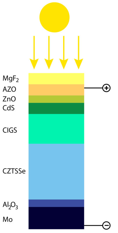
Scientists led by Pennsylvania State University in the U.S., however, suggest a different approach that could eliminate much of this complexity. In a paper published in Applied Physics Letters, they theorize that stacking two absorber layers into one cell, rather than stacking two full cells on top of each other, could result in both impressive efficiency achievements and low production costs.

Image: Pennsylvania State University
For such a device to work, the two absorber layers have to have quite a similar structure. The group at Penn State modeled such a device incorporating both copper-indium-gallium-selenide (CIGS) and copper-zinc-tin-sulfide/selenide (CZTS) layers into one cell, noting that these two materials have a similar lattice structure and can be deposited using the same vapor deposition techniques. Their optoelectronic models showed that with optimization of bandgaps in both layers, such a device could achieve 34.45% efficiency.
Popular content
For now though, this is only a theory. The group carried its modeling based on an ideal CZTS cell calculated to have 21.74% efficiency – , which could be described as a little optimistic compared to what has so far been achieved with this material at the lab scale.
“Fabrication of this double-absorber thin-film solar cell, or an approximative variant thereof, will require the attention of experimentalists for careful compositional grading and may not perform as well as predicted by a detailed optoelectronic model,” the group concludes. “Nevertheless, this solar cell is promising for ubiquitous in-device microwatt-scale generation of electricity.”
This content is protected by copyright and may not be reused. If you want to cooperate with us and would like to reuse some of our content, please contact: editors@pv-magazine.com.


By submitting this form you agree to pv magazine using your data for the purposes of publishing your comment.
Your personal data will only be disclosed or otherwise transmitted to third parties for the purposes of spam filtering or if this is necessary for technical maintenance of the website. Any other transfer to third parties will not take place unless this is justified on the basis of applicable data protection regulations or if pv magazine is legally obliged to do so.
You may revoke this consent at any time with effect for the future, in which case your personal data will be deleted immediately. Otherwise, your data will be deleted if pv magazine has processed your request or the purpose of data storage is fulfilled.
Further information on data privacy can be found in our Data Protection Policy.