From pv magazine USA
Leading Edge Equipment Technologies – a startup making manufacturing equipment to produce kerfless, single-crystal silicon wafers for solar panels – just closed a $7.6 million series A financing round.
The round was led by Prime Impact Fund, Clean Energy Ventures along with DSM Venturing. Previous investors in the startup include Applied Materials, Clean Energy Venture Group and David Buzby.
The company’s technology falls in the kerfless wafer or direct-wafer category. Kerfless production does not require silicon ingots to be sawn into wafers, a time- and energy-consuming multi-step process which uses consumables and wastes material as silicon dust. According to the company, its “drop-in” manufacturing technology cuts wafer costs by 50%, increases commercial solar panel power by up to 7%, and reduces manufacturing emissions by more than 50%.
Rick Schwerdtfeger joined Leading Edge as CEO and Nathan Stoddard joined as CTO earlier this year. Prior to this funding round, the startup secured $1.45 million in angel and venture funding, according to Pitchbook. It has also received $4 million in US Department of Energy funding. Founder and board member Alison Greenlee, with previous experience at kerfless silicon wafer startup 1366 Technologies, is the chief product officer.
Ribbon solar
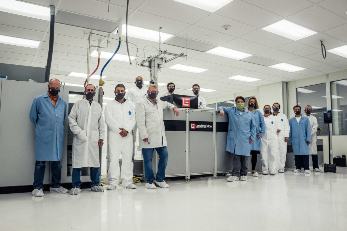
The company’s product is a new type of silicon wafer production furnace.
“The furnace is actually producing a single crystal — basically a one-wafer-wide ribbon that comes out of the furnace, and then is laser cut at the furnace into sections,” CEO Rick Schwerdtfeger told pv magazine. “And those sections can be further laser-cut or cleaved into net shape wafers with no need for diamond sawing and saw damage removal etching – and no need for the traditional cropping and all the challenges of taking a very large CZ boule and turning it into thin wafers. We grow basically a net shape wafer coming out of the furnace.”
Popular content

The “Floating Silicon Method” process was pioneered by Leading Edge founder Peter Kellerman while at Varian Semiconductor, which was later acquired by Applied Materials for $4.9 billion back in 2011.
Schwerdtfeger, the CEO, said the “dirty little secret” of solar power is the energy intensity and emissions in the purification and forming of the silicon materials. “Our process wastes virtually no silicon – and that has a major impact on factory emissions,” he said.
Other startups have gone down the kerfless road and have had limited success. Twin Creeks and SiGen attempted to manufacture kerfless silicon using ion-implantation. Crystal Solar and Ampulse were working gas-to-wafer technology. Evergreen Solar was a publicly listed ribbon solar company. These companies are now defunct, but 1366 Technologies is still alive and forming wafers directly using molten silicon.
Leading Edge’s customers are the solar module incumbents and perhaps some hungry upstarts challenging those incumbents. The startup CEO said he looks to have “furnaces into the field by late next year.”
Schwerdtfeger told pv magazine that the reason he took this job was because “this is the most disruptive innovation I’ve seen in silicon in the last 30 years – and I have to be part of it.”
This content is protected by copyright and may not be reused. If you want to cooperate with us and would like to reuse some of our content, please contact: editors@pv-magazine.com.


What does this indicate for your results of our analysis?