Scientists from Jinan University in China have used selective nanosecond-pulse, laser-induced ablation to fabricate a perovskite solar module with a reduced heat-affected zone.
“Considering the conversion efficiency and the recent progress in the accelerated stability measurement, we believe that it is time to start the mass production of this type of solar modules,” researcher Yaohua Mai told pv magazine. “To our knowledge, there are already tens of startup companies which are involved in the perovskite PV manufacturing. Microquanta, a company based in Zhejiang province, China, has rolled out a square meter size prototype. In addition, we recently set up a new company and started to build a pilot line and then a commercial production line.”
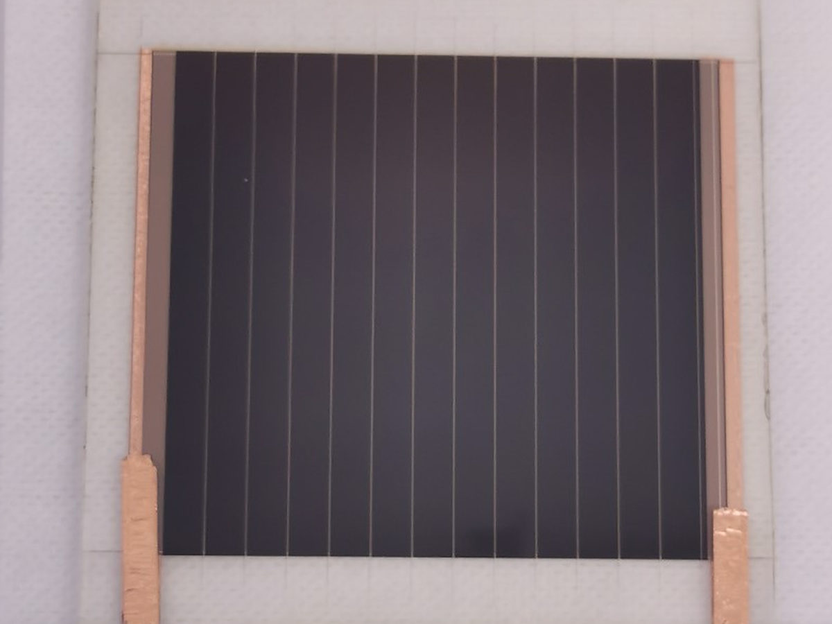
The research team used inverted perovksite cells with a p-i-n structure for the panel. These cells have an efficiency of 22.16%,an open-circuit voltage of 1.15 V, a short-circuit current of 23.23 mA cm−2, and a fill factor of 0.83. The scientists divided the cells into an array of sub-cells that are interconnected in series. This configuration is intended at achieving a high voltage and low photocurrent device, which should result in lower resistive losses.
The researchers built the cells with a transparent conductive oxide (TCO) substrate, a hole transport layer (HTL) the perovskite layer, an electron transport layer (ETL), and a silver (Ag) metal contact. They interconnected the solar cells via P1, P2, and P3 scribes.
“We used a 30 ns laser with a wavelength of 1064 nm to scribe P1 because a wide band gap indium tin oxide (ITO) has free carrier absorption in the near-infrared region,” the scientists said noting that the high pulse-to-pulse overlap is used in P1 patterning to obtain clean and smooth scribe line valleys. “In the P2 patterning step, the perovskite layer, as well as other functional layers are removed to construct interconnections between the sub-cells. In the P3 step, the top electrode is removed along with all other layers except the ITO, to exclude shunting of adjacent sub-cells of the device.”
Popular content
The academics described the manufacturing process based on the nanosecond laser as “good enough” to obtain the high-quality interconnection for perovskite solar modules.
“The champion perovskite solar module yielded a certified aperture efficiency of 21.07% and a geometric fill factor of 95.5%, which is one of the highest reported so far,” they concluded. “This result leads the way to further simplification and reliability in perovskite solar module production.”
They presented the details of the module tech in “Can Nanosecond Laser Achieve High-Performance Perovskite Solar Modules with Aperture Area Efficiency Over 21%?” which was recently published in Advanced Energy Materials.
This content is protected by copyright and may not be reused. If you want to cooperate with us and would like to reuse some of our content, please contact: editors@pv-magazine.com.


2 comments
By submitting this form you agree to pv magazine using your data for the purposes of publishing your comment.
Your personal data will only be disclosed or otherwise transmitted to third parties for the purposes of spam filtering or if this is necessary for technical maintenance of the website. Any other transfer to third parties will not take place unless this is justified on the basis of applicable data protection regulations or if pv magazine is legally obliged to do so.
You may revoke this consent at any time with effect for the future, in which case your personal data will be deleted immediately. Otherwise, your data will be deleted if pv magazine has processed your request or the purpose of data storage is fulfilled.
Further information on data privacy can be found in our Data Protection Policy.