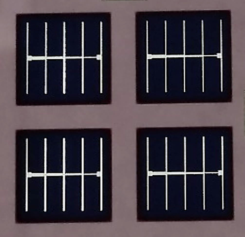
Researchers from Tokyo City University have fabricated a germanium (Ge) heterojunction solar cell with an area of 1 square centimeter, which they claim is the highest level ever reported for the technology thus far.
“The Ge heterojunction solar cell was developed as the bottom cell of the triple-junction solar cell,” researcher Makoto Konagai told pv magazine. “Concrete applied research is a future theme. It could be used as a detector in the infrared region or a light-emitting device in the infrared region.”
One of the biggest issues with Ge solar cells is cleaning the Ge wafers from impurities and reducing their reflectance.
“For Ge wafers, unlike silicon, there is no known simple texture etching method to reduce the surface reflectance,” the scientists said.
With this in mind, they built the cell with a magnesium fluoride (MgF2) as an anti-reflecting coating and an 80-nanometer indium tin oxide (ITO) substrate with antireflection properties. They said the two layers were able to increase the cell short-circuit current.
Popular content
The researchers also used a passivation layer based on n-type doped hydrogenated amorphous silicon (n-a-Si:H), a 317 μm thick p-doped Ge wafer that went through hydrofluoric acid (HF) and hydrochloric acid (HCl) treatment, a buffer layer made of a-Si:H, another ITO substrate, and a silver (Ag) metal contact.
“In heterojunction Ge solar cells, the surface treatment of wafers and the passivation of the n-a-Si:H / p-Ge interface are very important,” they said, noting that both the HF and HCl treatments are key to increasing open-circuit voltage. “In addition, by increasing the thickness of the i-a-Si:H layer on the low resistivity substrate, the solar cell characteristics tended to improve in all parameters.”
They tested the Ge solar cell under standard illumination conditions. It achieved an efficiency of 8.6%, an open-circuit voltage of 291 mV, a short-circuit current of 45.0 mA/cm2, and a fill factor of 0.656.
“At present, Ge wafers are expensive, so we are not at the stage of discussing the cost yet,” Konagai said. “Since the manufacturing cost is high, it is crucial to increase the conversion efficiency to reduce the power generation cost.”
This content is protected by copyright and may not be reused. If you want to cooperate with us and would like to reuse some of our content, please contact: editors@pv-magazine.com.


1 comment
By submitting this form you agree to pv magazine using your data for the purposes of publishing your comment.
Your personal data will only be disclosed or otherwise transmitted to third parties for the purposes of spam filtering or if this is necessary for technical maintenance of the website. Any other transfer to third parties will not take place unless this is justified on the basis of applicable data protection regulations or if pv magazine is legally obliged to do so.
You may revoke this consent at any time with effect for the future, in which case your personal data will be deleted immediately. Otherwise, your data will be deleted if pv magazine has processed your request or the purpose of data storage is fulfilled.
Further information on data privacy can be found in our Data Protection Policy.