From pv magazine USA
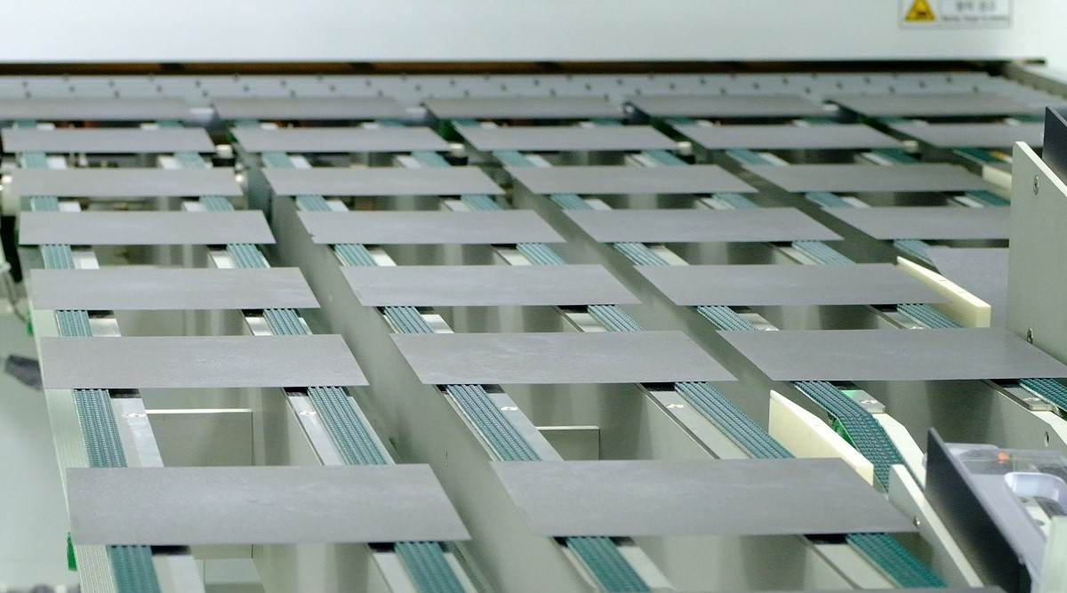
CubicPV has announced plans to establish 10 GW of conventional mono wafer capacity in the United States. Driven by incentives in the Inflation Reduction Act, the wafers produced by the new facility could fill a void in the domestic supply chain, while also creating 1,500 new direct jobs.
“The IRA represents a titanic shift in the global solar landscape, and the U.S. is poised to become the world’s most competitive location to manufacture solar,” said Frank van Mierlo, CEO of CubicPV. “We’re excited to have a role in the U.S. manufacturing renaissance while accelerating our business plan and supporting the development of our next generation tandem module technology.”
CubicPV was formed last year from the merger of 1366 Technologies and Hunt Perovskite Technologies. 1366 Technologies was known for its direct wafer technology, which forms wafers directly with molten silicon. The advantage is that kerfless wafer production does not require silicon ingots to be sawn into wafers – a time-consuming process that wastes materials such as silicon dust. Instead, the company’s technology forms wafers directly, using molten silicon.
Texas-based Hunt Perovskite Technologies, which was founded in 2013, specializes in metal halide perovskite in single-junction solar panels for the utility-scale market. The merger has therefore resulted in a new production process that combines 1366’s direct wafer process and Hunt’s printed perovskite solar photovoltaic technology.
Popular content
While CubicPV reports that its new factory will produce conventional silicon wafers, it said it will continue research and development of its tandem modules, which reportedly offer more than 30% greater efficiency than the highest-efficiency conventional modules. The design stacks two solar cells, with silicon on the bottom, powered by CubicPV’s Direct Wafer technology and perovskite on the top, to “dramatically increase the power of every acre of solar deployed,” according to the company.
CubicPV has not yet chosen a site for its US facility, but it says the design has begun. It expects to finalize the site choice in the first quarter of 2023. Construction is anticipated to be completed in 2024, with the factory fully ramped up in 2025.
“The Solar Energy Manufacturers for America (SEMA) Coalition applauds CubicPV for bringing the first global-scale wafer manufacturing facility to the United States,” said Mike Carr, the executive director of the Solar Energy Manufacturers for America (SEMA) Coalition. “Their planned 10 GW facility to manufacture conventional mono wafers will serve as a major catalyst in our efforts to create a fully American solar supply chain.”
To continue reading, please visit our pv magazine USA website.
This content is protected by copyright and may not be reused. If you want to cooperate with us and would like to reuse some of our content, please contact: editors@pv-magazine.com.


2 comments
By submitting this form you agree to pv magazine using your data for the purposes of publishing your comment.
Your personal data will only be disclosed or otherwise transmitted to third parties for the purposes of spam filtering or if this is necessary for technical maintenance of the website. Any other transfer to third parties will not take place unless this is justified on the basis of applicable data protection regulations or if pv magazine is legally obliged to do so.
You may revoke this consent at any time with effect for the future, in which case your personal data will be deleted immediately. Otherwise, your data will be deleted if pv magazine has processed your request or the purpose of data storage is fulfilled.
Further information on data privacy can be found in our Data Protection Policy.