PEDOT:PSS/silicon solar cell built at room temperature with 10.1% efficiency

Scientists from Kyoto University in Japan have developed an organic-inorganic hybrid HJT solar cell without using vacuum or high-temperature processes. They used PEDOT:PSS, a polymer known for its low cost and easy preparation properties, as a hole transport layer in a silicon (Si) heterojunction cell.
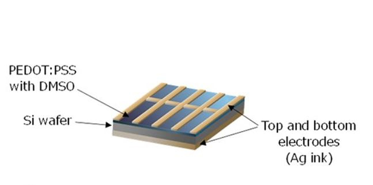
To form electrodes without using costly processes like screen printing, electroless plating, and vacuum evaporation, the academics employed a highly conductive silver (Ag) ink agent to coat the semiconductor materials as the electrodes. Their solar cell fabrication process thus comprised only three coating processes: coatings of a PEDOT:PESS layer on a bare Si wafer, of a top Ag electrode on the PEDOT:PSS layer, and of a bottom Ag electrode on the back surface of the Si wafer.
The researchers then explored the optimal process condition and sequence that maximizes the solar cell performance. They found the best results for cells fabricated using first a wet hydrofluoric acid treatment to remove the native oxide layer on the Si surface, then the coating on the back of Si wafer, followed by submerging the Si wafer in deionized water, then coating the PEDOT:PSS layer, and finally coating the top of the wafer.
Following this process, the team said it found “a drastic change in the cell efficiency on the submerging time [of the wafer in deionized water,] where too shallow or intense oxidation of the top Si surface severely degrades the cell.” The scientists found the optimal time period for this process to be one minute and the ideal rotation velocity for the spin coating of PEDOT:PSS to be 5,000 rpm.
A lab-scale 8 mm2 cell fabricated under these conditions showed a conversion efficiency of 10.1%, an open-circuit voltage of 0.57 V, a short-circuit current density of 33.3 mA/cm2, and a fill factor of 0.53.
The academics said the efficiency value is far from the state-of-the-art PEDOT:PSS/Si HJT solar cells “due to severe restriction of the process condition … The low fill factor severely limiting the efficiency is attributed to the relatively high series resistivity.”
Nevertheless, the scientists noted that their fabrication approach “may lead to convenient, low-cost, high-throughput photovoltaic device manufacture, particularly beneficial for the use in the developing countries and educational sites.”
They shared their findings in “An all ambient, room temperature-processed solar cell from a bare silicon wafer,” which was recently published in PNAS Nexus.
This content is protected by copyright and may not be reused. If you want to cooperate with us and would like to reuse some of our content, please contact: [email protected].

Please login to comment