Having made rapid progress optimizing their active cell materials, researchers working on perovskite PV devices are turning their focus to the other important layers that make up a PV device, and the interfaces between these, to further improve on performance.
All-back contact (ABC) cell architectures – where both the electron transport layer and the hole transport are deposited on the rear side of the cell – have shown performance advantages in silicon PV, though increased processing costs compared to other silicon cell types mean they are only a niche product in rooftop PV markets.
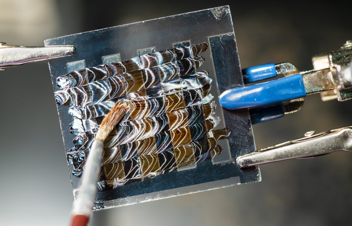
A group of scientists led by the US Department of Energy's National Renewable Energy Laboratory (NREL) decided to test the ABC structure in perovskite devices, reasoning firstly that the absence of a front contact layer can increase efficiency by allowing more light to reach the perovskite layer, secondly that they open up new possibilities for front side passivation and encapsulation – potentially improving device stability, and finally that they allow for the use of in-situ techniques to analyze the device during operation.
At the interface
The group noted, however, that having both layers on the same side also comes with a host of challenges. They were able to fabricate ABC perovskite cells with an efficiency of just over 10%, representing a significant improvement over the previous 4.4% achieved in October 2020. Focusing on the interface between transport layers was key to this, a process of UV ozone exposure followed by annealing at 300 Celsius degrees was shown to both reduce defect density in the hole transport layer, and remove contaminants from the electron transport layer, increasing voltage, and current collection.
Popular content
After fabricating the cells, the group used sophisticated imaging and modeling techniques to find out where the performance losses occur and how they could be prevented, with this they were able to provide a pathway to achieving efficiencies beyond the 20% mark. The work is described in full in the paper Complementary interface formation toward high-efficiency all-back-contact perovskite solar cells, published in Cell Reports Physical Science.
Modelling suggests that focus on defects at the layer interfaces, the work function of the hole selective contact, and frontside passivation will be the best strategies to bring ABC cell efficiencies to 20% or better.
This content is protected by copyright and may not be reused. If you want to cooperate with us and would like to reuse some of our content, please contact: editors@pv-magazine.com.


1 comment
By submitting this form you agree to pv magazine using your data for the purposes of publishing your comment.
Your personal data will only be disclosed or otherwise transmitted to third parties for the purposes of spam filtering or if this is necessary for technical maintenance of the website. Any other transfer to third parties will not take place unless this is justified on the basis of applicable data protection regulations or if pv magazine is legally obliged to do so.
You may revoke this consent at any time with effect for the future, in which case your personal data will be deleted immediately. Otherwise, your data will be deleted if pv magazine has processed your request or the purpose of data storage is fulfilled.
Further information on data privacy can be found in our Data Protection Policy.