As laboratory work on perovskite solar cells continues to demonstrate impressive results, scientists are switching the focus to achieving those same results with techniques that can be applied in large-scale manufacturing.
Most of the highest-performing perovskite solar cells produced by researchers to date have been fabricated using spin coating, which is difficult to apply to larger surface areas. Other solution-based techniques such as inkjet printing, blade coating and slot-die coating have strong potential for low cost, high throughput manufacturing, but also tend to see high-performance losses as the device area increases. Many are investigating controlling these processes via additives to the precursor materials, but other routes could also be possible.
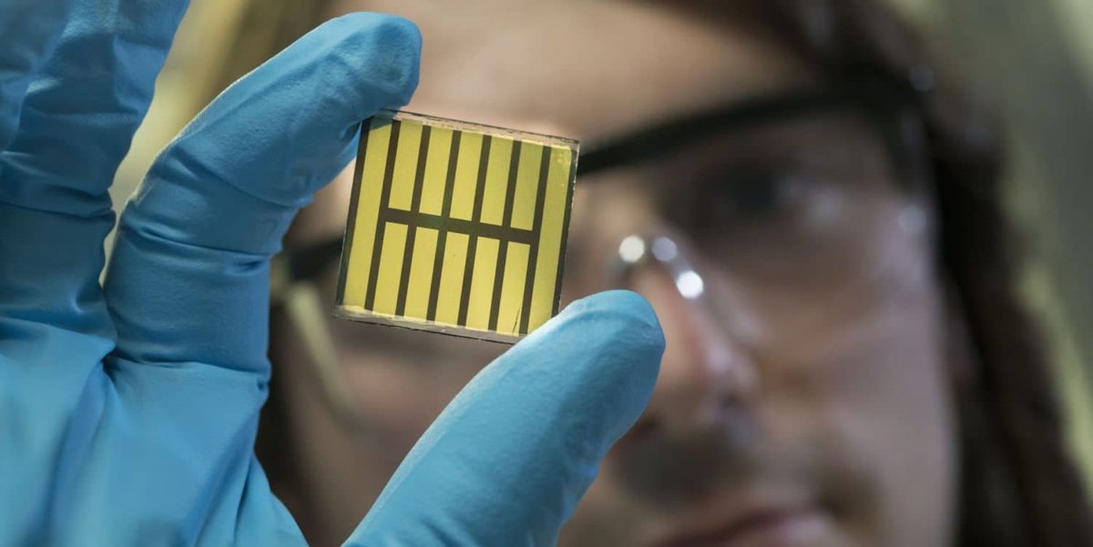
Scientists led by the Karlsruher Institute of Technology (KIT) in Germany investigated vapor-based deposition techniques for deposition of the cell layers, along with laser scribing for cell interconnections – both of which are established processes used in the production of other thin-film solar cells – CIGS or CdTe for example.
The group claims its work represents the first time these two techniques have been investigated in combination for a perovskite PV module, and demonstrates some encouraging results: They fabricated a 4cm² device that achieved 18% efficiency, and scaled this up to 51cm², reaching 16.6% efficiency.
Popular content
The techniques are described in full in the paper Upscaling of perovskite solar modules: The synergy of fully evaporated layer fabrication and all-laser-scribed interconnections, published in Progress in Photovoltaics. “The comparison of the achieved upscaling losses of only 3.1% (relative efficiency)/dec of upscaled area with other upscaling approaches as well as established thin-film PV technologies like CIGS, c-Si, and CdTe highlights the excellent upscaling efficiency of the developed process,” says the group.
They note that while initial efficiencies for perovskite cells fabricated with vapor-based deposition are lower than for solution-based, the vapor processing has lower losses associated with the increase in area. And regarding the laser processed interconnections, the results were achieved using a 532 nanosecond laser already suitable and established for industrial use, while other studies have relied on much more expensive and complex short-duration lasers.
This content is protected by copyright and may not be reused. If you want to cooperate with us and would like to reuse some of our content, please contact: editors@pv-magazine.com.


By submitting this form you agree to pv magazine using your data for the purposes of publishing your comment.
Your personal data will only be disclosed or otherwise transmitted to third parties for the purposes of spam filtering or if this is necessary for technical maintenance of the website. Any other transfer to third parties will not take place unless this is justified on the basis of applicable data protection regulations or if pv magazine is legally obliged to do so.
You may revoke this consent at any time with effect for the future, in which case your personal data will be deleted immediately. Otherwise, your data will be deleted if pv magazine has processed your request or the purpose of data storage is fulfilled.
Further information on data privacy can be found in our Data Protection Policy.