Laser-patterned poly-Si finger contacts reduce parasitic absorption, improve efficiency in TOPCon solar cells

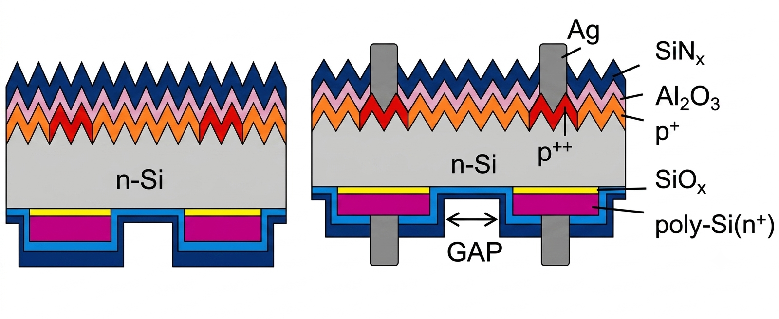
Researchers from China’s Yangzhou University have developed a laser-modification–assisted wet-etching process to fabricate rear poly-finger contacts for industrial TOPCon solar cells.
“Our work proposes a manufacturable poly-finger rear patterning strategy combining picosecond laser modification and precision potassium hydroxide (KOH) wet etching to boost the efficiency of industrial n-type TOPCon solar cells,” corresponding author Qinqin Wang told pv magazine.
The scientists explained that double-sided passivating contact solar cells suffer from parasitic absorption in front poly-Si layers and grid-line shadow losses, limiting efficiency improvements. Back-contact (BC) solar cells overcome these issues by placing passivating contacts on the rear side, eliminating front shading and approaching the theoretical efficiency limit of silicon cells. However, BC fabrication remains challenging due to complex rear-side patterning and precise metallization alignment, they emphasized.
They also noted that laser processing provides a promising approach for improving TOPCon solar cell performance by enabling precise and localized modification of the poly-Si layer. Partial removal of poly-Si can effectively reduce parasitic absorption losses, but excessive removal may compromise surface passivation and hinder carrier transport. In contrast, maintaining a continuous poly-Si layer preserves excellent electrical properties but leads to higher optical losses due to unwanted absorption.
With this in mind, the academics proposed a poly-finger structure that offers a practical balance between these competing effects by selectively retaining poly-Si beneath the metal contacts, where it supports efficient carrier collection, while removing poly-Si from non-contact regions to minimize parasitic absorption.
The new poly-finger structured was tested with n-type silicon wafers that were first textured using KOH-based alkaline etching to form light-trapping pyramidal surfaces, followed by boron doping and laser-based selective emitter formation. The rear surface was then polished, and a silicon oxide (SiOx)/poly-Si passivating contact stack was deposited by low-pressure chemical vapor deposition (LPCVD) and annealed to form doped poly-Si.
A picosecond green laser was then used to selectively remove rear SiOx/poly-Si regions, followed by KOH wet etching to create poly-Si gaps in unmetalized areas. Front and rear surface passivation layers were deposited before screen-printing silver electrodes and firing to complete the solar cell fabrication.
The fabricated devices were characterized through electrical, optical, and structural measurements, including I–V testing, implied open-circuit voltage, saturation current density, contact resistivity, microscopy analysis, and reflectance measurements. These characterizations were used to evaluate the effects of laser modification and wet etching on morphology, passivation quality, carrier transport, and optical losses.
The analysis showed that increasing KOH cleaning time increased the gap height while improving uniformity, with an optimal condition of 480 s that achieved the best open-circuit voltage, fill factor, and carrier lifetime. Short etching times caused incomplete and uneven poly-Si removal, whereas excessive etching introduced edge roughening and recombination losses.
The laser energy density controlled the modification depth, providing the best balance between effective removal and minimal damage, according to the research team. Higher laser energies increased affected depth but degraded passivation due to residual damage and reduced carrier transport. The optimized process reportedly improved precursor passivation and reduced recombination losses, while the optimized poly-Si removal increased short-circuit current by eliminating non-contact poly-Si absorption.
Tested under standard illumination conditions, the champion cell built with this configuration achieved a power conversion efficiency of 26.08%, an open-circuit voltage of 746.1 mV, a short-circuit density of 14,014 mA, and a fill factor of 83.6%. The results were certified by Germany’s Institute for Solar Energy Research Hamelin (ISFH).
“Optimized laser overlap ratio, energy density and alkaline etching time deliver uniform gap structures, lifting implied open-circuit voltage and short-circuit current density while introducing slight fill factor decline owing to aggravated lateral carrier transport resistance,” Wang explained. ” Our scalable laser-assisted rear patterning route provides a practical solution for high-efficiency industrial passivated-contact silicon solar cells.
The analysis was upported by TCAD and Quokka 3 simulations, which clarified the trade-off between optical gain and electrical transport loss determined by gap width, the researchers said.
Their findings are available in the study “Laser-assisted poly-finger rear patterning for efficiency enhancement in industrial n-TOPCon solar cells,” published in Solar Energy Materials and Solar Cells.
This content is protected by copyright and may not be reused. If you want to cooperate with us and would like to reuse some of our content, please contact: [email protected].

Please login to comment