Solvent-free perovskite-silicon tandem solar cell achieves 27.3% efficiency

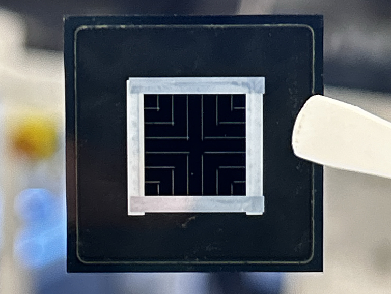
Researchers from the University of Freiburg and the Fraunhofer Institute for Solar Energy Systems (Fraunhofer ISE) in Germany have fabricated a perovskite-silicon tandem solar cell using a fully solvent-free manufacturing process.
“At the heart of the project is the fabrication of the perovskite layer using physical vapor deposition (PVD) and other solvent-free, industrially scalable processes,” the scientists said in a statement. “The perovskite layer was deposited through sequential evaporation.”
PVD offers a solvent-free approach to thin-film deposition, as the coating material is transferred directly to the substrate through the vapor phase under vacuum, eliminating the need to dissolve the material in a liquid carrier. The approach can also reduce solvent-related contamination and eliminates the need for subsequent solvent removal or drying steps.
“We have succeeded in eliminating all solvents from the manufacturing process of the wide-bandgap perovskite top cell and integrating this technology into the world’s first fully solvent-free perovskite-silicon tandem solar cell,” said lead author Mohamed A. A. Mahmoud.
“Thanks to excellent collaboration with researchers from four different countries, we were able to combine various measurement techniques to gain a detailed understanding of the processes taking place during the deposition of the perovskite thin films,” said co-author Juliane Borchert. “Perovskite-silicon tandem solar cells have great potential to become the next generation of highly efficient solar cells. For them to make the transition from the laboratory to industrial manufacturing, it is essential to identify the optimal combination of deposition methods that enables reliable, large-scale, and high-throughput production. With this solvent-free tandem solar cell, we are laying an important foundation for achieving this goal.”
The researchers built the solvent-free device in a monolithic two-terminal (2T) configuration, with a sequentially evaporated perovskite top cell integrated onto a silicon heterojunction (SHJ) bottom cell. They deposited the perovskite absorber via sequential evaporation using an optimized precursor recipe designed to achieve the required bandgap and complete conversion of the lead-halide precursors.
The scientists also deposited the hole-transport layer (HTL) by evaporation, avoiding solution processing at the bottom interface of the perovskite cell. At the upper interface, they deposited an ethylenediammonium diiodide (EDAI) passivation layer, followed by a 15-nm buckminsterfullerene (C60) electron-transport layer (ETL). They then deposited 20 nm of tin oxide (SnOₓ) via atomic layer deposition (ALD) and 25 nm of indium tin oxide (ITO) by sputtering.
The 1 cm² device was completed with a 200-nm silver (Ag) electrode and a 100-nm magnesium fluoride (MgF₂) layer.
Tested under standard illumination conditions, the tandem cell achieved a power conversion efficiency of 27.1%, an open-circuit voltage of 1,903 mV, a short-circuit current density of 19.3 mA/cm², and a fill factor of 73.8%. The device also retained 97.06% of its initial efficiency after 6,800 hours of storage in the dark under a nitrogen (N₂) atmosphere.
The scientists said in situ X-ray diffraction (XRD) measurements provided insights into the growth and conversion of sequentially deposited perovskite absorbers on planar and textured silicon substrates. They found that textured silicon promoted more effective conversion of lead-halide precursors into the perovskite phase than planar silicon.
The researchers also observed halide redistribution during thermal annealing, highlighting the importance of carefully optimized annealing conditions for achieving high device performance. However, they noted that the elevated processing temperatures impose additional thermal-stability requirements on the hole-transport layers.
“This achievement and the new insights into the crystallization processes form an important foundation for the further optimization of the technology and its future industrial implementation,” the academics concluded.
The new manufacturing process was described in “Impact of silicon substrate topography on sequentially evaporated perovskite film growth,” published in Joule.
This content is protected by copyright and may not be reused. If you want to cooperate with us and would like to reuse some of our content, please contact: [email protected].

Please login to comment