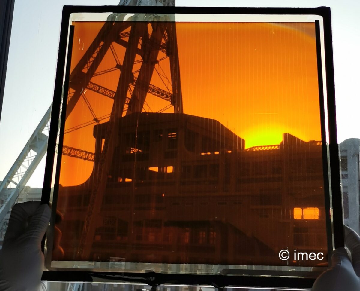
A research team led by Imec, a Belgian research institute, has fabricated a perovskite solar module based on a scalable device stack.
“We report the development of a stable device architecture that can be processed with industry-compatible techniques, such as sputtering, evaporation, and slot-die coating,” researcher Anurag Krishna told pv magazine.
The panel is based on 17%-efficient perovskite solar cells built with a p-i-n configuration, an electron transport layer made of nickel(II) oxide (NiOx), a perovskite layer deposited via slot-die coating, an electron transport layer made of buckminsterfullerene (C60) and lithium fluoride (LiF), a bathocuproine (BCP) buffer layer, and a copper (Cu) electrode.
The scientists constructed a 56-cell monofacial panel with an active area of 784 cm2, a power conversion efficiency of 13.08%, and a geometrical fill factor (GFF) of about 89%. They then built a second bifacial module by replacing the Cu electrode with one based on indium tin oxide (ITO).
“Under thermal and light stress, the electrode metals like Cu, Au, Ag, etc. are known to diffuse into the perovskite layer and thus compromise long-term stability, whereas devices with transparent conductive electrodes have shown much better stability under accelerated aging,” they explained. “The ITO has lower conductivity as compared to metal electrodes, which can lead to resistive losses and consequently a lower fill factor. To minimize that, we created a module design with reduced subcell width leading to 93 subcells.”
The bifacial panel has an aperture area of 781 cm2 and is able to achieve a power conversion efficiency of 11.9%.
Popular content
“Moreover, the encapsulated bifacial mini-modules (4 cm2) developed exhibited high tolerance to the IEC 61215-based damp heat [85 C, 85% relative humidity (RH)], the best ones retaining around 92% of initial efficiency after 1,000 hours,” Krishna said, noting that interfacial passivation could further increase the efficiency of the device.
The researchers said the results show that the proposed device stack is thermally stable, and that encapsulation is robust enough to ensure stability.
The academics presented the module in “Stable Device Architecture With Industrially Scalable Processes for Realizing Efficient 784 cm2 Monolithic Perovskite Solar Modules,” which was recently published in IEEE Journal of Photovoltaics.
“This work is an important milestone in the development of up-scalable manufacturing technologies for perovskite photovoltaics,” said Krishna.
This content is protected by copyright and may not be reused. If you want to cooperate with us and would like to reuse some of our content, please contact: editors@pv-magazine.com.


2 comments
By submitting this form you agree to pv magazine using your data for the purposes of publishing your comment.
Your personal data will only be disclosed or otherwise transmitted to third parties for the purposes of spam filtering or if this is necessary for technical maintenance of the website. Any other transfer to third parties will not take place unless this is justified on the basis of applicable data protection regulations or if pv magazine is legally obliged to do so.
You may revoke this consent at any time with effect for the future, in which case your personal data will be deleted immediately. Otherwise, your data will be deleted if pv magazine has processed your request or the purpose of data storage is fulfilled.
Further information on data privacy can be found in our Data Protection Policy.