There is no doubting the potential of heterojunction (HJT) PV. A relatively mature technology that can deliver 23%-plus cell efficiencies, it is well suited to bifaciality and exhibits an excellent temperature coefficient in the field. On the manufacturing front, there are also advantages. HJT requires fewer process steps than other high-efficiency concepts – four fewer than passivated emitter rear contact (PERC); it is a low-temperature process and therefore well suited to thinner wafers, and has a relatively small footprint.
Given these performance and production factors, the case for cell manufacturers to adopt HJT appears, on paper, to be a no-brainer. However, there has been a noticeable lag in companies turning to HJT, and for the production equipment suppliers providing tools for the critical manufacturing processes, the wait for more widespread adoption must seem interminable.
Meet HJT
Heterojunction with intrinsic thin-layer cell technology, to use the full name, was pioneered by Japanese electronics company Sanyo some 20 years ago – which had begun developing solar cells in the 1970s. In 2011 Panasonic completed its acquisition of Sanyo and continued the HIT activities. The Japanese company refers to the technology as HIT – a registered trademark.
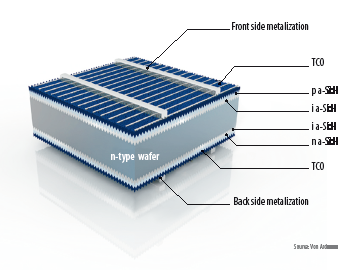
The cell architecture involves depositing two very thin amorphous silicon (a-Si) layers, one intrinsic and one doped, onto both sides of the c-Si wafer. The first, intrinsic a-Si layer passivates the c-Si, with this step a key factor in achieving high performance, while the doped layers create the p-n device structure. A transparent conductive oxide layer (TCO), often indium tin oxide, due to its transparency and conductivity, is then deposited onto the a-Si.
For some 13 years, Sanyo and then Panasonic produced high efficiency HIT cells and modules, under patent protection. During that period efficiencies have increased impressively. In 1997 HIT cell efficiencies, rolling off production lines, stood at 16.4%. That number rose to 19.3% by 2007, and 22.2% today. Panasonic kicked off 2017 by announcing that it had produced 18 million HIT modules over two decades – and has since upped its warranty protection, in the European marketplace, to 25-years. It points to a temperature coefficient of -0.258%/C, delivering superior production in warmer climes when compared to conventional PV technology.
New marketplace
In 2010, the patents protecting Panasonic’s HIT technology expired, opening the way for equipment suppliers and manufacturers to begin working with the technology, and providing solutions to the market. The patent expiry spurred a wave of activity, both from PV equipment vendors and other production technology providers from related industries such as semiconductor or flat panel production – particularly in the key HJT process steps including PECVD, PVD, and wet chemistry. But still the flow of HJT manufacturing projects, particularly at scale, has resembled more of the trickle than a flood.
“There’s not very much interest,” comments independent solar analyst Corrine Lin, when reporting on the uptake of HJT amongst Chinese cell producers. She says that only a hand full of larger Chinese PV cell manufacturers are currently producing HJT. A notable exception to this is Jinergy, which announced in April that it had begun mass production of its bifacial HJT modules. Jinergy announced it is achieving cell efficiencies of 23% and temperature coefficient of -0.28%/°C.
Production challenges
“The patents are down, but building it [an HJT fab] up is more than just setting-up the equipment. Strong technology know-how and feasible partners are necessary to collaborate with too,” says Kristin Lüdemann, the VP of crystalline silicon PV for equipment supplier Von Ardenne. The German tool making company has a long track record, of some 20 years, in supplying vacuum sputtering equipment for thin film PV production, most notably to CdTe giant First Solar. Von Ardenne entered the crystalline silicon PV business about 10 years ago, and since then has supplied TCO deposition tools for HJT application of more than 1.5 GW of cell production capacity since that date.
Key challenges to TCO deposition in HJT production, Lüdemann says, is that the process itself must not influence the sensitive ultra-thin a-Si layers, and that the process temperature must not exceed 200°C, while combining best optical and electrical film properties. Von Ardenne offers both of its HJT dedicated systems SCALA, for R&D and pilot production, and XEA|nova, for high volume manufacturing, to the HJT community.
Lüdemann reports that over the last two-to-three years there has been growing interest in HJT, and that she is working with more than 30 prospective industry partners.
Process challenges
There are other technical challenges beyond the TCO. Manufacturers and their equipment partners must ensure that the wafer is appropriately prepared, the a-Si/c-Si junctions are optimized, that excellent surface passivation is achieved, and the TCO layer is uniform across cells and functions as intended. And, on a fab level, unlike PERC, one or two new tools cannot convert a standard back surface field (BSF) cell line to HJT.
“PERC has almost become the standard,” notes analyst Corrine Lin. “Everybody can do PERC, just by buying the same machine. But for some new entrants, if they want some differentiation with top players, they need to choose a different technology. HJT efficiency is higher than PERC, and it is easier than IBC [interdigitated back contact], so it’s a good choice for them.”
For HJT production, the c-Si wafer must undergo wet chemistry processing unique to the demands of the a-Si deposition. Wafer cleaning is crucial because if any contaminants or sub-surface saw damage are not removed from the wafer surface, it can lead to a compromised c-Si/a-Si interface.
The wafer texturing is also more demanding than in standard BSF production, with the wet chemical processing required to create “big pyramids” on the wafer surface, according to Singulus’ Jens Eckstein, who heads up the German company’s wet chemical equipment operations.
“For standard cells using the alkaline process that we have, the process times are six minutes,” says Singulus’ Eckstein. “Heterojunction requires a process time of between 12 and 16 minutes.” As a result of this, batch processing of wafers for HJT is currently preferred, although Eckstein says that it’s conceivable the inline wet chemical tools may be suitable in years to come, as processes continue to improve.
Dirk Beisenherz, responsible for PVD equipment notes that Singulus supplies its SILEX II wet chemistry bench, alongside a waste-water treatment solution, and its GENERIS PVD platform, an inline sputtering system, as a kind of ‘package deal’ for HJT producers. The German company reports that it has shipped several SILEX II systems to China, the U.S. as well as to Russian PV producer Hevel – assisting Hevel to convert its a-Si lines to HJT.
From a-Si to HJT
Indeed, a clear majority of a-Si producers, including the largest remaining producer Italy’s 3Sun, have decided to go down this route – given a-Si’s declining competitiveness. This de facto a-Si upgrade opportunity is an important one for the HJT equipment suppliers and will provide a proof-of-concept for the technology at scale.
Also working on the Hevel project is Switzerland’s Meyer Burger, which is the only equipment supplier at present supplying a turnkey HJT cell and module solution.
Meyer Burger operates an HJT pilot cell line, at its German operations in Hohenstein-Ernstthal, the former Roth&Rau facility – where it also produces its MAiA tools for PERC upgrades. The facility, an industrial-scale HJT cell line, brings together Meyer Burger’s ELiAPECVD and HELiAPVD tools, along with metallization, curing, and high-efficiency SpotLIGHT testing platform. In having this line on hand, Meyer Burger can and is working with prospective manufacturers on optimizing the deposition steps at scale – demonstrating a truly industrial HJT solution.
While Meyer Burger won’t disclose the precise number of cell producers with which it is carrying out qualification programs on HJT, it does say that there has been a significant shift in the level of activity in the space over the last 12-18 months.
“Potential customers have changed from being interested in evaluation, towards studying concrete project feasibility, and going into planning – particularly for greenfield projects,” says Meyer Burger CTO Gunter Erfurt. At present, Meyer Burger reports that it can process cells with a thickness of down to 135μm in high volumes and achieve efficiencies above 23%, on its Hohenstein-Ernstthal pilot line. The company has worked with sub 100μm wafers in R&D and says that even with such thin substrates, its PECVD and PVD processes can achieve excellent passivation, avoiding resistance challenges at the module level.
“We believe, and looking into wafer manufacturer roadmaps and their cost projections, you see wafer thicknesses approaching 120μm in the coming years, you need cell technology that can take it – and this is clearly possible with HJT and definitely not with PERC or PERT,” says Meyer Burger’s Erfurt.
Potential turning point
There is broad agreement among technology providers that a move by a large, tier-one PV cell manufacturer, particularly if it is Chinese, into HJT production will prove decisive if others are to follow suit. The question remains, and it is a great unknown within the solar industry, when will this occur?
“From our market feedback, the industry will jump towards HJT when we see efficiencies above 23% in the pilot stage customer lines across the board,” says Frank Jürgens, the director of sales and marketing for Swiss PECVD system manufacturer Indeotec. He says that this must be demonstrated on production lines with a capacity of at least 100 MW, with single tools matching this throughput. “But we are not talking about the pilot stage alone,” adds Indeotec CEO Omid Shojaei.
Indeotec was founded in 2011 and has supplied five of its Octopus II PECVD/PVD platform to research labs globally in that time. The technology startup has its roots in a-Si equipment provider Oerlikon and believes that its ‘mirror’ deposition technology, and its ability to ensure there is no cross contamination between the deposition of the intrinsic and doped a-Si layers, gives it an edge over more established solutions on the market. Indeotec’s ‘mirror’ PECVD reactor technology allows for the coating of both sides of the c-Si wafer without the need to flip the wafer nor break the vacuum, an approach that Von Ardenne can also carry out when applying the TCO layer.
While Indeotec has, to date, only supplied its Octopus II tool – which is a laboratory platform – it claims that its Octopus III will have a throughput well in excess of 3,000 wafers/hour and on a significantly reduced footprint, when compared to other solutions. While the Octopus II can deposit both the a-Si and TCO layers, the Octopus III will be a pure-play PECVD tool.
“Our goal is to achieve the PECVD conversion cost around $0.02/W,” says Indeotec CEO Shojaei. “Per wafer, this is a saving of $0.10/wafer, just because of the PECVD.” Indeotec will have completed a qualification facility at the former TEL Solar site in Switzerland this month and believes that despite its small size, it has the deposition technology know how and the “agile” business strategy required to push HJT technology into the market.
Asian technology equipment suppliers are also active in HJT development and Taiwan’s Archers already has the experience in delivering equipment for compatriot’s manufacturer NSP’s move into the high-efficiency cell concept. China’s Ideal Energy Equipment is collaborating with Von Ardenne. In July, Ideal Energy announced it had received “new orders… for mass production equipment” for an HJT line, although more details are not yet available.
Industry analyst Corrine Lin estimates that in 2017 around 1.5 – 2 GW of HJT product will roll off production lines globally, with that growing “just slightly” next year. She notes that while HJT modules can achieve a module power output of 330W, compared to 300W for mono PERC, the additional cost of production is around $0.15 – $0.20/W, compared to $0.03/W for a PERC upgrade.
The collaborations between equipment suppliers and the level of activity in pushing HJT forward holds great promise regarding reducing its production costs. As an example, Singulus reports that on the Hevel HJT project it was able to introduce ozone wafer processing, significantly reducing costs. The Singulus team describes HJT production as more like a semiconductor process, rather than PV, and says that approaches from this far larger industry can be applied – delivering significant cost savings.
Von Ardenne points to the ability to upsize its established XEA|nova platform, of which it has already supplied 11 tools to HJT manufacturers, to the much larger XENIA – massively increasing the number of wafers that can be processed in each batch.
Meyer Burger reports that due to its “fast process” it can achieve a throughput of 2,400 wafers/hour, “but of course you can cluster equipment and achieve increased throughput,” says CTO Gunter Erfurt. “And this is just the beginning, and how we enter the market, further throughput increases are clearly on our roadmap.”
This content is protected by copyright and may not be reused. If you want to cooperate with us and would like to reuse some of our content, please contact: editors@pv-magazine.com.
