Heterojunction solar cells could provide the next big efficiency leap in solar output, but their need for low processing temperatures means they require very high quality, expensive n-type silicon wafers.
In recent years, significant research has been devoted to eliminating defects in low-cost p-type silicon, so that it could start to match and perhaps surpass the cost-to-efficiency ratios of the long-time hero of the photovoltaic industry – PERC technology. However, a new review of research into defect engineering in p-type wafers could reroute the path to a silicon heterojunction takeover.
Although Australia has seen record uptake of rooftop solar, the upfront costs of solar systems remain a barrier to more widespread deployment. Engineering more efficient solar cells would mean households need fewer solar panels, with attendant lower installation costs, to meet their electricity needs. And homes with small roof expanses could get more bang per solar panel.
Recent research on the performance of cheap p-type silicon wafers has shown great promise. But Dr. Matthew Wright, a solar researcher at the University of New South Wales (UNSW), says in a newly published research paper that “the same techniques can be applied to n-type wafers to improve the performance of those cells.”
Wright is an Australian Renewable Energy Agency (ARENA) post-doctoral fellow in the UNSW School of Photovoltaic and Renewable Engineering (SPREE). He worked on the final stages of the four-year Hydrogenated and Hybrid-Heterojunction P-type Silicon Solar Cells project, led by UNSW Associate Professor Brett Hallam.
Wright and PhD student Bruno Vicari Stefani recently spoke to pv magazine Australia about their research, which is based on Stefani’s PhD paper on improving p-type silicon. They also considered the work of other UNSW scientists, including Dr. Anastasia Soeriyadi, as well as researchers from the Australian National University and Arizona State University. In addition, they considered results gleaned from manufacturers who are already incorporating some of these methods into production.
Foot in the door
Globally, a number of manufacturers are producing silicon heterojunction solar cells, including Hevel Solar. The Russian manufacturer produces 340 MW of silicon heterojunction cells per year, and claims an efficiency of 24.1%. Wright points to China's Tongwei Solar as another major silicon heterojunction manufacturer.
The thinking has been that if manufacturers could substitute cheap p-type silicon for the current standard use of n-type in silicon heterojunction production, while not sacrificing too much of the p-type efficiency, the tide of production and further development might swing toward silicon heterojunction, to give greater cost-to-efficiency benefits than PERC can now achieve. PERC (passivated emitter and rear cell) technology was invented by Professor Martin Green of UNSW in the early 1980s. Speaking at this year’s Smart Energy Summit, Green said that in 2021, around 95% of global silicon solar cell production will use p-monocrystalline PERC.
PERC already uses the cheaper p-type silicon because of the very high temperatures (around 700 C) used to form the electric field in the solar cell, says Wright. The high temperatures help to solidify the metal contact points, which are screen-printed onto the cells as a metal paste. This also has a positive, or passivating, effect on the quality of the silicon.
In silicon heterojunction cells, however, the material applied to the surface of the cells, which delivers their high-voltage efficiencies, is sensitive to heat. It cannot be subjected to greater than 200 C.
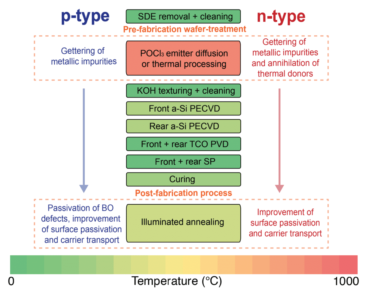
“So all those kind of defect-engineering approaches that are inherent in the PERC cell fabrication, and which improve the quality of the silicon are out the window,” says Wright. “The whole point of our review and the whole point of Bruno’s thesis, is to get around that problem by treating the wafer before it goes into making the cell, and doing some kind of annealing process after the cell is finished.”
In one example, researchers at UNSW are using high-intensity laser light in a process known as “illuminated annealing.” They use this method to change structures within the cells as a final stage of production.
The cost of such processes is outlined in “Progress with Defect Engineering in Silicon Heterojunction Solar Cells.” The paper was published in the 60th-anniversary edition of PSS Rapid Research Letters.
This content is protected by copyright and may not be reused. If you want to cooperate with us and would like to reuse some of our content, please contact: editors@pv-magazine.com.


2 comments
By submitting this form you agree to pv magazine using your data for the purposes of publishing your comment.
Your personal data will only be disclosed or otherwise transmitted to third parties for the purposes of spam filtering or if this is necessary for technical maintenance of the website. Any other transfer to third parties will not take place unless this is justified on the basis of applicable data protection regulations or if pv magazine is legally obliged to do so.
You may revoke this consent at any time with effect for the future, in which case your personal data will be deleted immediately. Otherwise, your data will be deleted if pv magazine has processed your request or the purpose of data storage is fulfilled.
Further information on data privacy can be found in our Data Protection Policy.