Scientists from the Dalian University of Technology in China have designed a tandem solar cell based on two PV devices both relying on kesterite (CZTSSe).
“Through our simulation, we improved the performance of the two cells by adjusting band alignment at interfaces, selecting proper buffer layers, and adding a double layer to both subcells,” the research's corresponding author, Bita Farhadi, told pv magazine.
In the study “Numerical modeling and performance analysis of a novel Cd-free all-Kesterite tandem solar cell using SCAPS-1D,” published in Next Materials, the research group said it used the SCAPS-1D solar cell capacitance software, developed by the University of Ghent, to simulate the novel cell configuration.
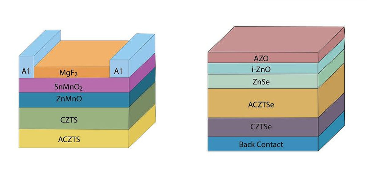
The researchers designed the upper cell with an aluminum (Al) layer, a buffer layer made of tin, manganese, and oxigen (SnMnO2), a kesterite absorber, a double layer of copper zinc tin sulfide (CZTS), and the nickel (Ni) metal contact. The lower cell was designed with an Al layer, an ultrathin aluminum-doped zinc oxide (AZO) film, a window layer of zinc oxide (i-ZnO), two layers of kesterite, and a Ni metal contact.
“The Mn-doped SnMnO2 is a suitable material for the window layer in thin film solar cells since it is affordable and environmentally benign,” the scientists said, noting this compound is replacing commonly utilized cadmium sulfide (CdS). “The modified solar cell performs better in terms of both short-circuit current and open-circuit voltage. These increments are not due to proper tuning of parameters but also to the correct collection of buffer and window layer with suitable band offset at the buffer/window interface.”
The group achieved the current matching between the subcells by adjusting the thickness of the CZTS absorber layer in the upper device. Furthermore, it introduced a second kesterite absorber layer in the lower device to mininimze the conduction band offset (CBO) and increase its open-circuit voltage.
Through the simulation, the academics found that the ideal thickness of the absorber in the upper subcell is 143.3 µm, while for the lower subcell they calculated a thickness of 1.5 µm. These sizes would result in an identical current density value of 20.29 mA/cm2.
Popular content
The champion tandem device designed via the simulation achieved a power conversion efficiency of 23.96%, an open-circuit voltage of 1.637 V, a short-circuit current of 20.29 mA/cm2, and a fill factor of 72.05%.
The upper cell was found to achieve an efficiency of 14.05%, an open-circuit voltage of 1.0 V, a short-circuit current of 20.29 mA/cm2, and a fill factor of 68.86%. The lower device reached an efficiency of 20.0%, an open-circuit voltage of 0.632 V, a short-circuit current of 20.29 mA/cm2, and a fill factor of 81.14%.
“Our tandem design with optimum band alignment at the ZnMnO/CZTS and ZnSe/CZTSe interfaces outperforms the previous design with a CdS/absorber structure and ZnS/absorber,” the academics stated. “These simulation results pave the way for selecting the best material combination and designing highly efficient kesterite single-junction and tandem solar cells.”
Kesterite is one of the most promising light absorber material candidates for potential use in lower-cost thin-film solar cells. Kesterites include common elements such as copper, tin, zinc, and selenium. Unlike CIGS compounds, there are no supply bottlenecks expected in the future.
However, kesterite is still less efficient than CIGS in mass production. The world record for such cells is 12.6%, achieved for large-area devices by Japanese thin-film producer Solar Frontier in 2013.
This content is protected by copyright and may not be reused. If you want to cooperate with us and would like to reuse some of our content, please contact: editors@pv-magazine.com.


2 comments
By submitting this form you agree to pv magazine using your data for the purposes of publishing your comment.
Your personal data will only be disclosed or otherwise transmitted to third parties for the purposes of spam filtering or if this is necessary for technical maintenance of the website. Any other transfer to third parties will not take place unless this is justified on the basis of applicable data protection regulations or if pv magazine is legally obliged to do so.
You may revoke this consent at any time with effect for the future, in which case your personal data will be deleted immediately. Otherwise, your data will be deleted if pv magazine has processed your request or the purpose of data storage is fulfilled.
Further information on data privacy can be found in our Data Protection Policy.