Solar generates zero-emissions energy, but concerns are rising regarding the environmental and resource impact of PV module production. In today's market, the focus has shifted to evaluating the overall carbon footprint of solar modules. This shift can be attributed to the increasingly apparent effects of climate change, coupled with concerns about environmental issues and human health, as well as resource scarcity.
Examining the carbon footprint of a solar module is a pivotal aspect of this evaluation, offering a concise metric for comparing production methods. Lower carbon footprint numbers signify production processes that demand fewer of the Earth's resources, reflecting a commitment to environmental sustainability.
Silicon demand
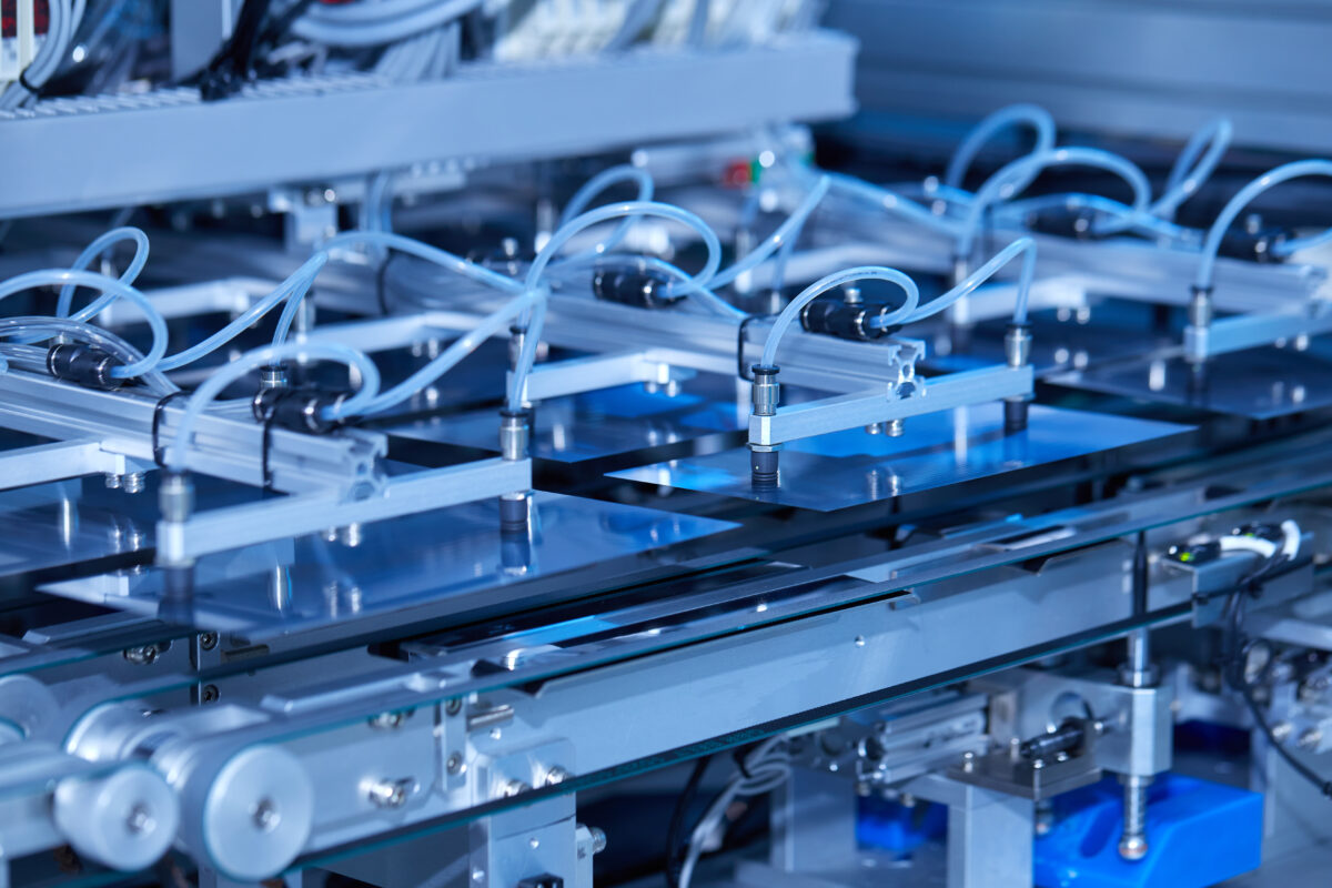
The process of manufacturing solar cells and wafers requires significant amounts of energy in a demanding series of processes. Technological breakthroughs are critical to help shift solar manufacturing’s use of resources into greener and greener territory.
A key energy demand for most types of popular PV products is the production of polysilicon, which requires high temperatures to refine to the purity necessary for the silicon wafers used in solar. The process involves heating quartz sands in a furnace. The polysilicon is then formed into ingots, which are cut and sliced into silicon wafers for use in crystalline products. The solar industry’s silicon demands are high, and solar products generally need in excess of 99.9999%, known as 6N purity. This is much higher purity than metallurgical silicon.
The latest solar manufacturing using crystalline silicon incorporates either the mature process known as passivated emitter and rear contact (PERC), and two newer processes or technologies known as tunnel oxide passivated contact (TOPCon) or HJT solar cell technology. Each manufacturing process has its own benefits for different stakeholders, and comparing and contrasting each technology process is beyond the scope of this article.
When solar modules are evaluated by traditional metrics, elements including efficiency, cost, and reliability are typical benchmarks. However, the carbon footprint of a module is an increasing focus for many stakeholders, and already subject to regulation by many countries, including France and Korea. In crystalline solar, which the industry’s supply chain is largely focused on, only one manufacturing technique has a far cleaner production process: HJT.
Comparing carbon
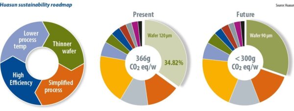
In July 2023, Huasun Energy released a carbon footprint report for its HJT solar module, the Himalaya Series G10-144, with the report certified by TÜV Rheinland. The HJT module saw a result of 366.12 g of CO2 equivalent emissions per watt. This makes it one of the first verified solar modules falling below the 400 g/W CO2 equivalent mark, and sees it fall into an industry category considered as ultra low-carbon solar.
The difference compared to other technologies is stark. While each manufacturer’s own carbon footprint will depend on the local electricity mix used in the complete production process, broad ranges have been established by industry reports. A Fraunhofer ISE study presented at 2022 World Conference on Photovoltaic Energy Conversion in Milan published details that imply a typical glass-glass solar module made in China, where more than 85% of the world’s PV manufacturing takes place, has a carbon footprint of around 750 g/W CO2 equivalent. That means Huasun’s latest module has almost half the carbon emissions.
HJT advantages
Huasun’s HJT module uses silicon wafers with a thickness of 120 micrometers. That compares to a typical thickness of 150 micrometers in other crystalline silicon technologies like PERC, thereby delivering big savings on the raw, energy intensive material. In addition, Huasun CTO Wang Wenjing explained that HJT technology is, on the whole, more friendly to the silicon wafer: more of the ingot can be used. Primarily, that’s because other technologies cut a solar cell after it’s made, whereas HJT tech uses a half wafer before the solar cell is made, meaning a smaller segment of wafer is taken from an ingot.
“In the past, when we cut a square ingot from a cylindrical ingot, the edge part was sent back to the CZ [Czochralski] furnace to be reformed into another ingot. But with the HJT cell, we can cut the edge part to get half-Si pieces. So we can use the edge part … to get more wafer pieces from the same ingot,” said Wang. This results in both cheaper silicon wafers and more efficient use.
The energy savings from HJT go further than the wafer thickness savings and efficient use of ingots. HJT uses low-temperature manufacturing processes and a simpler production process.
Huasun brands the process a “four-step” approach, and includes clearing and texturing, bifacial chemical vapor deposition (CVD), bifacial physical vapour deposition (PVD), and a final screen printing step. At each stage, the energy requirement is lower than 200 C – drastically lower than the 800 C to 1000 C required by other solar modules. For example, the process used in TOPCon technology may take as many as 10 or more steps. In addition, lower temperatures result in fewer cracks and defects, boosting both the yield of the production process and efficiency.
This article appears in the new Huasun Corporate Edition, launched on April 10, 2024. Read the whole edition here.
This content is protected by copyright and may not be reused. If you want to cooperate with us and would like to reuse some of our content, please contact: editors@pv-magazine.com.

By submitting this form you agree to pv magazine using your data for the purposes of publishing your comment.
Your personal data will only be disclosed or otherwise transmitted to third parties for the purposes of spam filtering or if this is necessary for technical maintenance of the website. Any other transfer to third parties will not take place unless this is justified on the basis of applicable data protection regulations or if pv magazine is legally obliged to do so.
You may revoke this consent at any time with effect for the future, in which case your personal data will be deleted immediately. Otherwise, your data will be deleted if pv magazine has processed your request or the purpose of data storage is fulfilled.
Further information on data privacy can be found in our Data Protection Policy.