The adoption of black silicon technology is now a major trend in the PV industry, with several tier-1 manufacturers operating gigawatt-scale capacities, and process and equipment suppliers reporting strong interest in the technology.
Black silicon can offer a range of benefits to module manufacturers: “What I am seeing is that not all black silicon is created equal, and people see it very differently,” explains Chuck Provini, President & CEO at Natcore. “At one level it is used for its anti-reflective properties, others are using it merely for its texturing function, and some are interested in it simply because it’s black and it looks pretty.”
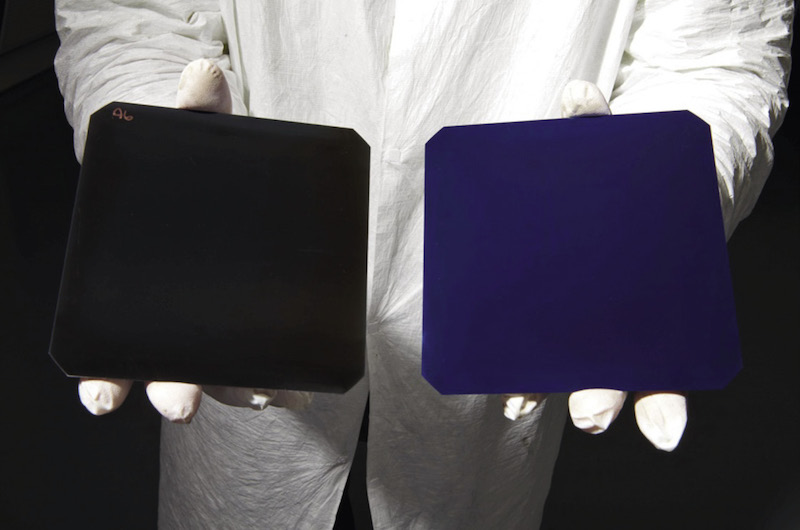
Natcore, a U.S.-based company that holds the license for a black silicon process originally developed by NREL, says that its main interest lies in the technology’s anti-reflective properties: “Anti-reflectivity is its primary function,” says Chief Technology Officer Dennis Flood. “With NREL, we created a silicon surface with an average reflectance of 0.5%, most solar cells have reflectance of between 3 and 6%.”
While surface reflectivity is an important factor in boosting cell efficiency, this alone has not proved enough to excite the PV manufacturing industry, and it is the texturing function of black silicon, and its potential as a solution to enable diamond wire sawing in multicrystalline wafer production, which seems to have played the largest role in black silicon’s recent popularity among cell and module manufacturers. “Diamond wire sawing is being introduced into multi wafer cutting nowadays, which can enable further increases in cell efficiency,” explains Xusheng Wang, Senior Director of Technical Integration at Canadian Solar. “With these new technologies, black silicon cells can have strong competitiveness in the market.”
Texturing multi c-Si
The adoption of diamond wire sawing has been a major factor in solar’s recent price drops. Thanks to problems in cutting multi wafers using diamond wire, this also brought about a shift towards monocrystalline silicon among PV manufacturers – according to IHS Markit, mono had a 31% market share in 2016, and is expected to reach 34% in 2017 – and set equipment providers the task of finding a viable solution to allow manufacturers to realize further cost cutting through diamond wire cut multi c-Si.
When multi is cut with diamond wire, the surface left behind is too smooth for standard texturing processes to be effective. Black silicon processes can give the required texture to a wafer’s surface, with the added bonus of reflectivity levels as low as 0.5%, slight increases to cell efficiency, and the elimination of other expensive production stages, including anti-reflective coating. Thanks to this, the technology now has the attention of several major module manufacturers.

Image: Natcore
“Black silicon is a hot topic in the solar industry right now, all of the cell makers are trying different ways to integrate it into mass production,” says Wang. “Canadian Solar has become the first company to turn all of its multi cell capacity (more than 4 GW) over to black silicon. In industrial production we have been able to achieve 19% average efficiency.”
Another top 10 module manufacturer, GCL Systems Integration (GCL SI), is also putting faith into black silicon processes, having announced the achievement of 20.78% peak cell efficiency using the technology, at the recent EU PVSEC conference held in Amsterdam. “In the future we think that diamond wire, plus multi, plus PERC black silicon – this combination of technologies should be the direction for us,” says Dong Shuguang, Executive President at GCL SI.
A tale of two processes
Two types of process for the creation of black silicon are already in use at commercial scale. Metal assisted chemical etching (MACE), which is a wet chemical process, and reactive ion etching (RIE), a dry process utilizing plasma. The difference between the two is that MACE leaves the surface of the silicon intact in a smooth, polished state, and drills thousands of nanoscopic pores into it, whereas RIE processes actually etch away most of the material on the surface of the wafer, and leave behind an inverted cone structure, the tips of each cone measuring just a few nanometers and up to a couple of hundred nanometers at their base.
The two processes can create cells that behave quite differently, particularly with the low angles of light typical in the morning and evening. According to Natcore’s Flood, however, these are of little significance once the cell is placed under module glass. “The glass controls what happens at those low angles of incidence,” he explains. “Our experience is, when the cell goes under glass in a normal module construction, you still get enhanced performance, but the angular advantages tend to wash out because of the glass’s very smooth surface.”
RIE is the more expensive process, but its costs can still be absorbed by the savings achieved through diamond wire sawing. Canadian Solar currently has the world’s largest black silicon capacity with a MACE wet etching process. GCL SI, on the other hand, is continuing to experiment with both processes, and has achieved the highest efficiencies using RIE.
The majority of GCL SI’s black silicon capacity, however is with an MACE process, and most analysts see these as more likely to become the dominant process as the technology matures. “80% of our capacity is MACE. This technology is what we are invested in today,” says Dong. “Another 20% of what we do is RIE, which we also use to make black silicon.”
Xusheng Wang of Canadian Solar adds that while the processes can be quite easily added to existing production lines, black silicon is far from being a mature production technology. “The equipment, processes, and chemical additives are not mature yet”, says Wang. “There are not yet any standard process details, and there is also no mature production equipment.”
No conflict
Both of the manufacturers that pv magazine spoke with for this article said that black silicon processes are cost effective and can easily be added to existing production capacities. “Black silicon deals with front side texturing and has no conflicts with other technologies like diffusion, passivation, or metallization,” continues Wang. “What’s more, black silicon can be used with PERC, which makes multi-PERC much more compatible in comparison with mono-PERC.” It will have to compete, though, with other technologies which allow diamond wire sawing for multicrystalline wafers. Such a process was, for example, presented by the German manufacturer Schmid earlier this year (see pv magazine March, page 62).
With adjustments to the conditions, either of the commercial black silicon processes could be used for mono c-Si as well as multi. Wang estimates that by itself, black silicon can provide a 0.4% efficiency boost alongside an unspecified cost reduction. “If you take it further, in optimizing the cell process then you also get gains in the filling factor of the cell and also the open circuit voltage increases,” adds Bill Rever, cofounder and Chief Marketing and Sales Officer at Advanced Silicon Group, a consulting company which itself has a proprietary metal etching process for black silicon.
This by itself has thus far not proved a sufficiently tantalizing prospect for the large-scale manufacturers to take note, and it is the potential for mainstream, low cost multi-PERC technology that drives the adoption of black silicon in the PV industry. “Our plan is to provide products including multi-PERC with glass-glass, bifacial modules,” concludes GCL SI’s Dong. “I think that this is one of the very good products that can bring a lot of value to our customers.”
This content is protected by copyright and may not be reused. If you want to cooperate with us and would like to reuse some of our content, please contact: editors@pv-magazine.com.
