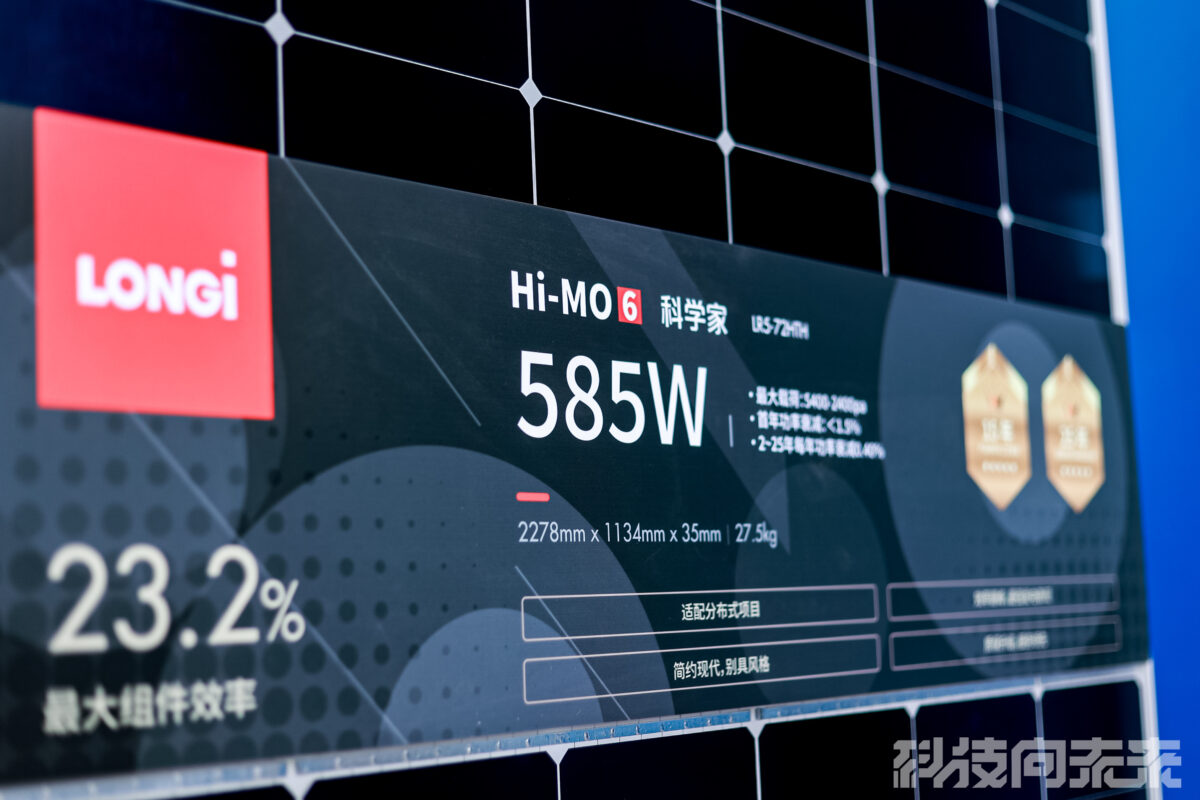
Chinese solar module manufacturer Longi plans to implement its back-contact solar cell technology in most of its panel production, as announced by the company's chairman, Zhong Baoshen, during an investor meeting last week.
“Longi has a very clear view that in the next five to six years, back-contact cells will be the mainstream of crystalline silicon cells,” he said. “The high conversion efficiency of BC cells is the crown jewel of crystalline silicon technology, and the whole industry is ready now to pick this jewel.”
Longi plans to achieve a total solar cell production capacity of 110 GW by the end of 2023, with 30 GW dedicated to TOPCon technology and 80 GW for BC technology.
Baoshen stated a preference for BC cells over TOPCon devices, on claims that TOPCon cell technology is transitional and offers minimal efficiency improvements compared to past PERC technology advancements.
Additionally, BC technology can be combined with p-type wafers, for which Longi has substantial production capacities, giving it an advantage over the more common interdigitated back-contact (IBC) technology.
“The back-contact (BC) cell technology improves photoelectric conversion efficiency by shifting all the electrode grids on the front side to the back side of the cell, thus reducing the shading of the grids from sunlight.” Shen Wenzhong, secretary general of the Shanghai Solar Energy Association and Director of the Solar Energy Research Institute at Shanghai Jiaotong University, told pv magazine. “As a cell structure, BC technology can be combined with a variety of cell technologies to form back-contact based solar cells.”
In March, Longi launched its own hybrid passivated back contact (HPBC) tech. The company has yet to explain exactly what HPBC is, but it is believed to be an extension of p-type (positively doped silicon) IBC technology that combines the structural advantages of PERC, TOPCon, and IBC solar.
Longi will develop “P-IBC” cells using its extensive production capacity of p-type wafers, along with a silicon dioxide tunneling layer, polysilicon film, and upgraded laser equipment, low-pressure chemical vapor deposition, and coating-cleaning equipment—all derived from PERC-process lines.
This content is protected by copyright and may not be reused. If you want to cooperate with us and would like to reuse some of our content, please contact: editors@pv-magazine.com.


Aren’t back contact cells already manufactured by other companies like Sunport Power “zero lead” panels and Sunport Powers “MWT” copper backcontact panels?
PV 100MW, Inverter on/of grid(All in one solution with PV, Battery, grid and load integrated)-50Kw, 2000pcs, Inverter on grid 5KW, 2000pcs, Battery deff cycle.(OPZV) 2V, 250AH, 480000pcs. Total prise?