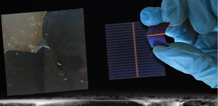
Researchers from Hangzhou Dianzi University in China have fabricated a thin film p-type monocrystalline solar cell that they claim may reach a power conversion efficiency approaching that of its industrial thick counterparts.
“Overall, the findings of this study present a novel way to realize high-performance thin crystalline silicon solar cells using much less silicon—for a 20-μm cell, around one eighth of the amount required for a thick 160-μm cell on a given panel size,” said researcher Leonidas Palilis.
In the paper “Investigation on significant efficiency enhancement of thin crystalline silicon solar cells,” published in the Journal of Photonics for Energy (JPE), the scientists explained that they used the layer transfer (LT) method instead of silicon ingot cutting for the production of the wafer used for the cell. LT is a technique to transfer a layer of a semiconductor material, often of a wafer-scale size, from the original substrate to the target substrate.
With this method, hydrofluoric (HF) acid is first used electrochemically to etch pores into a thick silicon wafer for porous silicon and this wafer is utilized as a substrate to epitaxially grow a monocrystalline silicon layer. The epitaxial thin silicon layer is then lifted off from the porous silicon substrate.
Via this process, the scientists obtained a p-type -thick thin monocrystalline silicon wafer. They then deposited multiple passivation layers made of aluminum oxide (Al2O3), silicon nitride (NiO2) and silicon monoxide (SiOx) via Plasma Enhanced Chemical Vapor Deposition (PECVD) at the front of the cell.
These contacts have two different configurations – SiO2/SiNx/SiOx and Al2O3/SiNx/SiOx – and reportedly improve light absorption in short wavelengths and longer wavelengths, which in turn enhances the cell short-circuit current and open-circuit voltage.
“Compared with a standard solar cell used as a reference, the current density increased from 34.3 mA/cm2 to 38.2 mA/cm2,” the academics said, adding that the passivation layers also contributed to raising the cell open-circuit voltage from 632 mV to 684 mV.
As a result, the device's fill factor increased from 76.2% to 80.8% and the cell efficiency grew from 16.5% to 21.1%.
”This advance will likely contribute to more widespread cost-effective adoption of silicon solar power technology, due to the reduced cost and the concomitant expansion of the solar panel manufacturing capacity,” said Palilis.
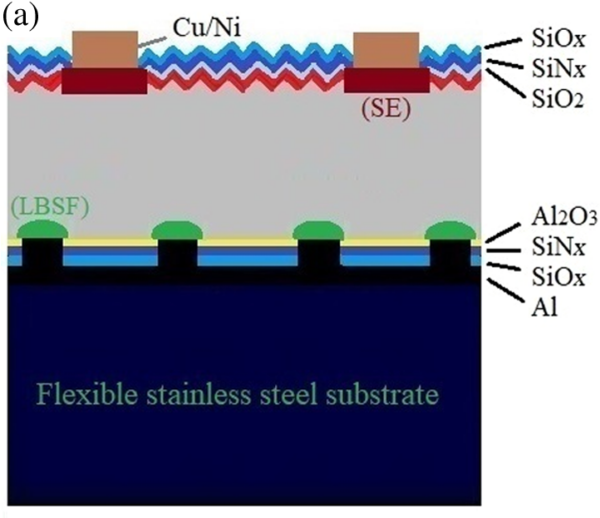
Image: SPIE - Society of Photo-Optical Instrumentation Engineers
This content is protected by copyright and may not be reused. If you want to cooperate with us and would like to reuse some of our content, please contact: editors@pv-magazine.com.


2 comments
By submitting this form you agree to pv magazine using your data for the purposes of publishing your comment.
Your personal data will only be disclosed or otherwise transmitted to third parties for the purposes of spam filtering or if this is necessary for technical maintenance of the website. Any other transfer to third parties will not take place unless this is justified on the basis of applicable data protection regulations or if pv magazine is legally obliged to do so.
You may revoke this consent at any time with effect for the future, in which case your personal data will be deleted immediately. Otherwise, your data will be deleted if pv magazine has processed your request or the purpose of data storage is fulfilled.
Further information on data privacy can be found in our Data Protection Policy.