Researchers at the University of Chicago (UChicago) and Cornell University claim they have developed a new method to make stacks of semiconductors that are just a few atoms thick.
According to a study published in the scientific magazine Nature, the new method may allow scientists and engineers to perform a simple, cost-effective procedure to make thinner semiconductor layers, which could come into use on devices ranging from solar cells to mobile telephones.
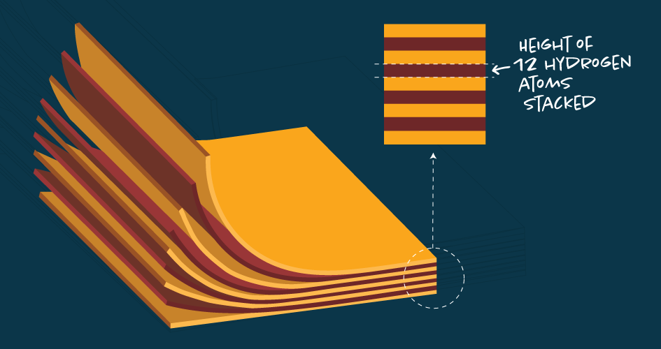
The research team said that the promising process, however, is still very delicate, as it leaves little room for error. “The scale of the problem we’re looking at is, imagine trying to lay down a flat sheet of plastic wrap the size of Chicago without getting any air bubbles in it,” said Jiwoong Park, a UChicago professor in the Department of Chemistry, the Institute for Molecular Engineering and the James Franck Institute, who led the study. “When the material itself is just atoms thick, every little stray atom is a problem,” Park added.
The scientists also said that the stacked films are detachable, suspendable and compatible with water or plastic surfaces, which will enable their integration with advanced optical and mechanical systems.
Compared to “grow” semiconductor layers, “stacked” layers have the advantage that these have not to be submitted to harsh growth conditions such as high temperatures. The U.S. research team, instead, puts the films into a vacuum, peels them off and sticks them to one another, “like Post-It notes”, Park said.
“The films, vertically controlled at the atomic-level, are exceptionally high-quality over entire wafers,” said the research’s co-author Kibum Kang.
The research team said it expects the new method to accelerate the discovery of novel materials, as well as enabling large-scale manufacturing.
This content is protected by copyright and may not be reused. If you want to cooperate with us and would like to reuse some of our content, please contact: editors@pv-magazine.com.


By submitting this form you agree to pv magazine using your data for the purposes of publishing your comment.
Your personal data will only be disclosed or otherwise transmitted to third parties for the purposes of spam filtering or if this is necessary for technical maintenance of the website. Any other transfer to third parties will not take place unless this is justified on the basis of applicable data protection regulations or if pv magazine is legally obliged to do so.
You may revoke this consent at any time with effect for the future, in which case your personal data will be deleted immediately. Otherwise, your data will be deleted if pv magazine has processed your request or the purpose of data storage is fulfilled.
Further information on data privacy can be found in our Data Protection Policy.