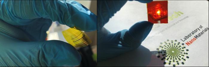
A research team including scientits from the laboratory of nanomaterials at the Skoltech Center for Photonics and Quantum Materials in Moscow, Estonia's Taltech University and the German Aerospace Research Center (DLR) claims to have developed a solar cell based on amorphous silicon with an efficiency of around 8.8%.
The achievement, the researchers said, was made possible by a novel p-type, flexible, transparent conductor made of carbon nanotube fibers which enabled the manufacturing of the amorphous cell at room temperature.
“We have progressed from the initial 1.6% and 3.4% reported previously, in 2016 and 2018, respectively, to 8.8% in 2019 using our newly developed p-type, transparent conductor for such hybrid thin film solar cells,” said Skoltech Ph.D student Pramod M. Rajanna.
Paper
The device is described in a paper published in Nano Energy. The scientists claim the performance marks an increase of around 16% on currently realized efficiencies for amorphous silicon solar. According to the ScienceDirect website, efficiencies for such devices sit at 6-7% and the theoretical limit for amorphous silicon cell efficiency is estimated at around 15%.
“We have developed a p-type transparent conductor with a state-of-the-art sheet resistance of 17 Ω/sq at a transmittance of 90% in the middle of the visible spectrum and a high degree of mechanical flexibility,” the research team stated.
The global market for amorphous silicon thin-film solar cells is likely to reach $5.31 billion by 2025, according to a report published by Singapore-based Energias Market Research Pvt. Ltd. “Traditionally, amorphous silicon thin-film solar cells were mainly used in small electronic devices due to their simplistic design and low efficiency,” stated the study. “However, with advancements in manufacturing techniques and an increase in their performance efficiency, these cells have found their application in building-integrated photovoltaics … the growing use of carbon nanotubes for charge transport between layers presents significant opportunity for the market.”
This content is protected by copyright and may not be reused. If you want to cooperate with us and would like to reuse some of our content, please contact: editors@pv-magazine.com.


It seems the transparent amorphous solar cell could be a window which would generate electricity and admit outside light to the interior at the same time?