Low-bandgap GaInNAsSb solar cell for multi-junction architectures


A research group from the Tampere University in Finland has developed a solar cell made of gallium-indium-nitride-arsenide-antimony (GaInNAsSb) that incorporates gold-based back-surface reflectors.
“This particular low-bandgap GaInNAsSb cell is developed to be used as part of lattice-matched multi-junction solar cells,” the research corresponding author, Riku Isoaho, told pv magazine. “Essentially these cells are meant to be used as the bottom junction in multi-junction architectures, absorbing the infrared wavelengths of the spectrum, boosting the efficiency of multi-junction devices that could then be employed in concentrated photovoltaics (CPV) for terrestrial power or in satellites for space applications.”
The cell has a “p-i-n” layout and an energy bandgap close to 0.8 eV. It was grown by molecular beam epitaxy (MBE), which is an evaporation technique implemented in an ultra-high vacuum for the deposition of compounds of extreme regularity of layer thickness and composition, and its structures were made with undoped GaInNAsSb absorber layers with a thickness of either 350nm or 700nm and a nitrogen concentration of around 6%, which were placed on a 210μm thick n-GaAs substrate. A four-layer anti-reflection coating (ARC) made of titanium oxide and silicon oxide (TiOx/SiOy) was deposited on the n-side of the cell using ion beam sputtering.
The performance of the device was assessed through external quantum efficiency (EQE) and light-current-voltage (LIV) measurements under standard solar illumination conditions. The EQE is the ratio of the number of energy carriers harvested by the solar cell to the number of photons of a given energy incident on the cell itself.
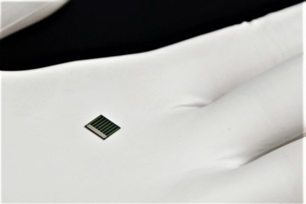
Image: Antti Tukiainen, Tampere University
The highest EQE, with a peak value of 0.79, was reported for a cell made with a 700nm GaInNAsSb absorber layer which also showed a lowest bandgap energy, of 0.78 eV. It also exhibited a short-circuit current density of 15.2 mA/cm2. According to the scientists, these values show the potential of low-bandgap GaInNAsSb to achieve current matching in advanced solar cells with five or more junctions.
“While the MBE production costs are generally higher compared to the commercial metal organic chemical vapor deposition (MOCVD) approach, when it comes to advanced solar cell concepts, such as multi-junction devices with four or more junctions, our approach has the advantage of being fully lattice-matched, enabling much thinner and simpler architectures compared with alternative technologies, which is expected to offset the MBE fabrication cost,” Isoaho further explained. “Moreover, we want to note that significant advances in the functionality, whether linked to superior efficiency, light weight, flexibility, or all, would reduce the sensitiveness of cost at cell level by enabling more advanced power systems.”
According to him, the building blocks for multi-junction devices implementing these low-bandgap subcells are already at a good level of maturity.”In order to fully assess their commercial potential, we need to complete full integration in five or six-junction architectures and then assess the performance for specific applications. In general, we are aiming for proof-of-concept level at this point.”
A complete description of the cell can be found in the paper “High performance low-bandgap (0.8 eV) single junction GaInNAsSb solar cells incorporating Au-based back surface reflectors,” published in Solar Energy Materials and Solar Cells.
The same research group unveiled, in March, a III-V multi-junction solar cell that is claimed to have the potential for reaching a power conversion efficiency of close to 50%.
This content is protected by copyright and may not be reused. If you want to cooperate with us and would like to reuse some of our content, please contact: [email protected].

Please login to comment