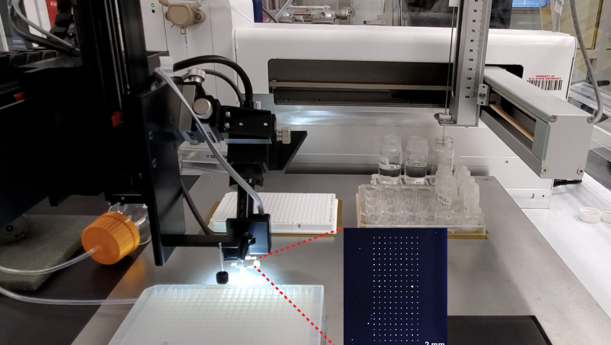
A team from North Carolina State University, Brookhaven National Laboratory, and Rey Juan Carlos University recently published the details of RoboMapper, a novel robotic materials discovery platform. The novel materials acceleration platform (MAP) can identify viable candidates for perovskite-silicon tandem solar cells.
“The target bandgap was ∼1.7 electron volt (eV) within mixed-cation, mixed-halide perovskites composition areas,” North Carolina State University researcher Aram Amassian told pv magazine.
The researchers validated new wide-bandgap compounds by analyzing RoboMapper-generated samples and spin-cast thin film samples, as well as through the fabrication of solar cells. They translated a predicted ideal compound, extensively detailed in the paper, into a champion device exhibiting an open-circuit voltage of 1.18 V, a short-circuit current of 21.54 milliampere per square centimeter, and a fill factor of 78.83%, for a 20% power conversion efficiency. The researchers said that devices with the new perovskite alloys show lower hysteresis and better photostability than other compounds evaluated at 1.7 eV.
It was important to the research team to demonstrate both environmental and productivity benefits.
“The RoboMapper can generate large datasets at a small fraction of the time, cost, and environmental impact of existing platforms, making it possible to develop new materials 10 times faster than traditional automation,” said Amassian. “There is a clear value proposition for anyone in the functional materials discovery space looking to do it competitively, responsibly, and sustainably.”
Amassian said that the team is actively pursuing partnerships to bring RoboMapper into commercial use. They have used the RoboMapper to define compositional boundaries, particularly where novel materials could demonstrate stability and efficiency. Amassian said RoboMapper's proficiency in this area could have implications for intellectual property in relation to new materials for PV, optoelectronics, and other functional applications.
The RoboMapper system uses a library of perovskite inks, which are perovskite film precursors or salts suspended in a solution, for easy deposition. It prepares the precursors inks, mixes, and loads the materials for deposition on chips (or substrates) for analysis and data collection.
The aspiration, mixing, and cleaning steps are automated. The samples undergo a battery of tests to evaluate the structure, bandgap, light stability, and level of suitability for PV applications. In parallel, the information is processed into models that are used to predict new perovskite compositions.
The tool can integrate hundreds of pixels per square centimeter, with an average pixel size of 50 micron diameter, according to the researchers. In this case, they palletized up to 150 compositions, with copies made for verification of reproducibility.
Amassian said there are several semiconductor-oriented mapping tools in development in academic and industrial research laboratories throughout the world.
“The prototyping platforms have applications in PV but also in printed electronics and other semiconductor applications in communications, displays, sensing and flexible electronics,” he added..
This content is protected by copyright and may not be reused. If you want to cooperate with us and would like to reuse some of our content, please contact: editors@pv-magazine.com.

1 comment
By submitting this form you agree to pv magazine using your data for the purposes of publishing your comment.
Your personal data will only be disclosed or otherwise transmitted to third parties for the purposes of spam filtering or if this is necessary for technical maintenance of the website. Any other transfer to third parties will not take place unless this is justified on the basis of applicable data protection regulations or if pv magazine is legally obliged to do so.
You may revoke this consent at any time with effect for the future, in which case your personal data will be deleted immediately. Otherwise, your data will be deleted if pv magazine has processed your request or the purpose of data storage is fulfilled.
Further information on data privacy can be found in our Data Protection Policy.