Researchers from the Fraunhofer Institute for Solar Energy Systems (Fraunhofer ISE) have developed new low temperature manufacturing processes for perovskite silicon tandem cells and heterojunction solar cells. The novel techniques are reportedly able to reduce silver consumption and avoid lead-containing soldering materials.
“We show that with a deep understanding of the processes and material behavior, low-temperature metallization and interconnection with the established equipment of solar cell and module production lines is possible,” the research's lead author, Angela De Rose, told pv magazine.
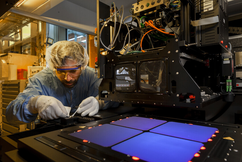
The scientists developed two different processes: front-side metallization at very low temperatures for full-size perovskite silicon tandem solar cells; and the interconnection to high-efficiency full-format demonstrator modules with an output power of more than 400 W.
The metallization step used fine-line screen printing. The selected paste was shown to be suitable for high-speed printing reliable at widths of 20 μm, resulting in a printed width of 26 μm. The process translated into 43% less silver consumption compared to a layout with finger widths of 35 μm. For curing at 150 C, “good electrical properties were reached” and high throughput production is possible due to fast curing times down to 2 minutes per wafer, according to the researchers.
For interconnection, the group used electrically conductive adhesives (ECA), screening several pastes and methods. “There are many commercially available ECAs on the market, allowing the processing at different temperature ranges, including less than 200 C and less than 150 C,” it explained, noting that most of ECAs use silver particles to ensure more electrical conductivity.
Their techniques achieved silver reduction by using finer line printing and less ECA than conventional methods and avoiding lead-containing materials in the low temperature screenprinting pastes and lead-free solder alloys.
The researchers claim they have been able to use 50% less ECA compared to the conventional continuous application patterns, noting that the proposed solution offers sufficient joint adhesion for string handling and stable module powers on the cells, also for ECA curing temperatures of 130 C. “The major challenge for this approach is to keep the curing time as short as possible to enable high throughput,” they said.
The solar modules made with a soldered wire interconnection and ECA ribbon interconnection have a total area of 1.8 m2, an output of more than 400 W, consisting of full-size perovskite silicon tandem half cells. The solder-coated wire enabled low-temperature processing and damage-free fabrication, said the researchers.
“By optimizing the involved processes and materials hand-in-hand, we were able to build highly efficient perovskite silicon heterojunction modules in full-format with different interconnection technologies,” said De Rose.
The team claimed the process enables high-throughput production at stringing speeds of 1600 to 1800 cells per hour. The cell matrix, either silicon heterojunction or tandem, was embedded into a commercially available encapsulant for a lamination process within a conventional process window between 140C and 160C. The full-size modules were built as glass-glass modules with edge sealing.
The processes were described in the study “Low-temperature metallization & interconnection for silicon heterojunction and perovskite silicon tandem solar cells,” published in Solar Energy Materials and Solar Cells.
The group’s future research activity includes lead-free and low-temperature soldering, shingling interconnection using ECA, as well as long-term stability of tandem cells and modules.
This content is protected by copyright and may not be reused. If you want to cooperate with us and would like to reuse some of our content, please contact: editors@pv-magazine.com.


By submitting this form you agree to pv magazine using your data for the purposes of publishing your comment.
Your personal data will only be disclosed or otherwise transmitted to third parties for the purposes of spam filtering or if this is necessary for technical maintenance of the website. Any other transfer to third parties will not take place unless this is justified on the basis of applicable data protection regulations or if pv magazine is legally obliged to do so.
You may revoke this consent at any time with effect for the future, in which case your personal data will be deleted immediately. Otherwise, your data will be deleted if pv magazine has processed your request or the purpose of data storage is fulfilled.
Further information on data privacy can be found in our Data Protection Policy.