First attempt to build back-contact micrometric III-V photovoltaic cells

Researchers at the Université de Sherbrooke in Canada have fabricated miniaturized back contact triple junction III-V solar cells that have a low shading factor and a high wafer area utilization.
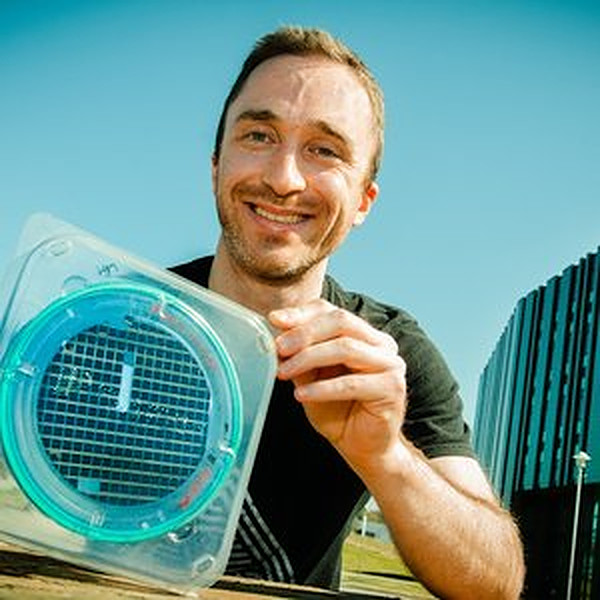
“We have developed triple-junction cells with a size twice the thickness of a strand of hair,” the research corresponding author, Matthieu De Lafontaine, told pv magazine. “The cells have significant advantages over conventional solar technologies, reducing electrode-induced shadowing by 95% and potentially lowering energy production costs by up to three times.”
According to De Lafontaine, those properties lend themselves to various applications, from the densification of electronic devices to areas such as solar cells, portable electronic devices, and lightweight nuclear batteries for space exploration, as well as miniaturization of devices for telecommunications and the internet of things.
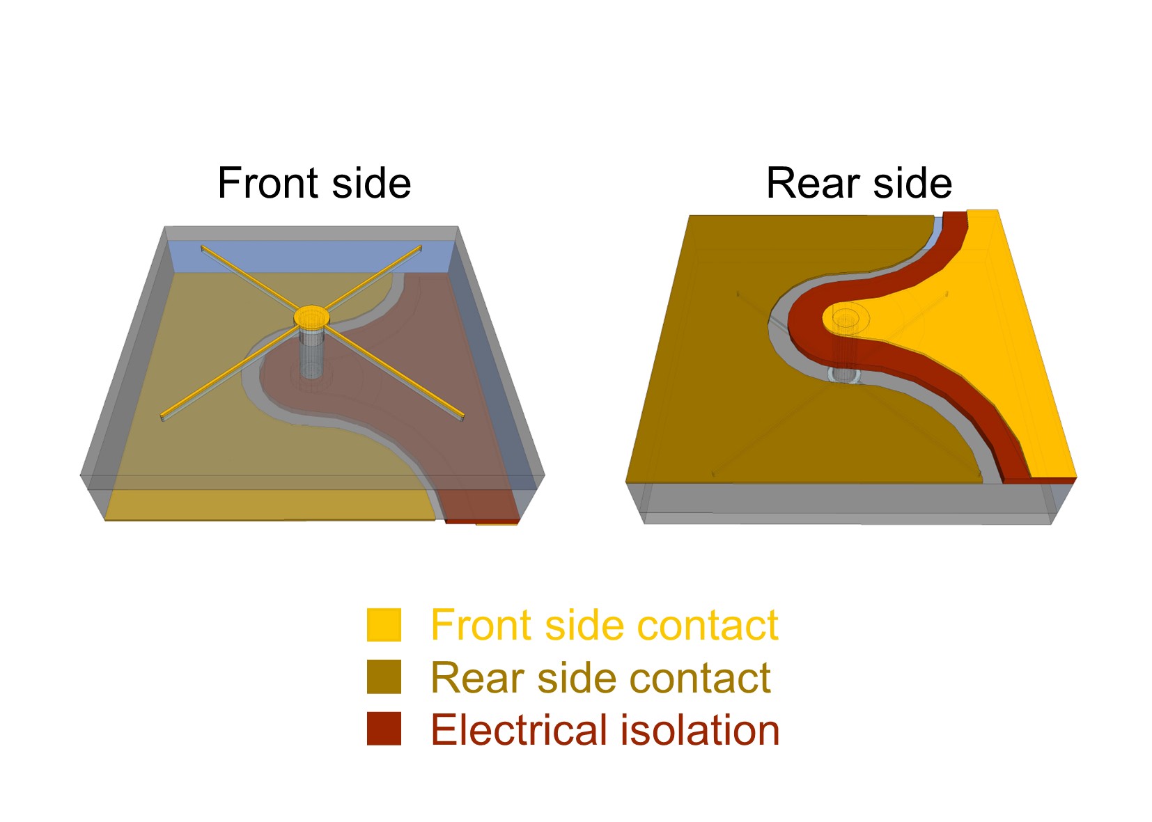
The scientists built the three-junction cells with three-dimensional (3D) interconnects based on through substrate vias (TSVs), which are commonly utilized to create 3D integrated circuits in micro-electromechanical systems. They consist of vertical electrical connections that pass completely through a silicon wafer.
“For photovoltaics, 3D interconnects can increase the conversion efficiency and reduce the shading,” they explained. “Using TSVs to transfer the front side contact to the back side through the device could mitigate shading, dark current contribution, and resistive losses.”
The group applied this new concept to triple-junction III-V solar cells, which are well known for strong performance and efficiency, but also for shading and resistive losses. “However, the baseline process does not depend on a specific heterostructure, which means that it could be applied to four or more junction solar cells,” they stated.
Moreover, the cost of producing cells made from III-V materials has confined them to niche applications, such as drones and satellites, where low weight and high efficiency are more pressing concerns than cost.
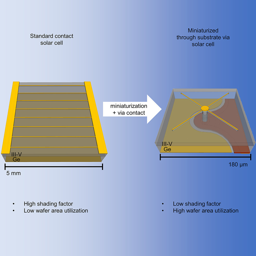
The cell is based on a top cell made of indium, gallium and phosphorus (InGaP), a middle device relying in indium, gallium and arsenide (InGaAs), and a bottom cell made of germanium (Ge). The scientists used wafer bonding to handle 20-μm-thin III-V films. They were able to reduce significantly the metallized area on the front side of the entire solar cell through the 3D interconnections.
Tested under standard illumination conditions, the cell achieved a power conversion efficiency of 18.3% an open-circuit voltage of 2.276 V, a short-circuit current density of 8.61 mA/cm2, and a fill factor of 82.1%.
The novel cell design was also found to achieve a small shading factor below 3% and a 6-fold increase in wafer area use, compared to cells based on 2D interconnects. “Simulation results have shown that TSVs could reduce the series resistance by 70% compared with standard contacts on triple-junction solar cells,” the group said.
The team includes academics from the Canada’s University of Ottawa and the Université Grenoble Alpes CNRS in France. They presented the device in the paper “3D interconnects for III-V semiconductor heterostructures for miniaturized power devices,” published in Cell Reports Physical Science.
“The development of these first back-contact micrometric photovoltaic cells is a crucial step in the miniaturization of electronic devices,” they concluded.
This content is protected by copyright and may not be reused. If you want to cooperate with us and would like to reuse some of our content, please contact: [email protected].

Please login to comment