Researchers at the University of Rajshahi in Bangladesh have made a new attempt to design solar cells based on a tin selenide (SnSe) absorber and claim their new solution may lead to the development of highly efficient devices.
“SnSe has innate p-type electrical conductivity which raises the possibility of using it as an absorber material in photovoltaic solar energy technology,” the scientists said, noting that this compound has so far reached low efficiencies in practical solar cell applications. “According to the Shockley-Queisser index, the maximum photovoltaic conversion efficiency for each type of SnSe structure is estimated to be around 32%.”
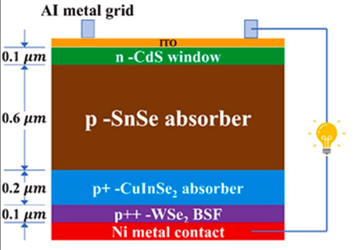
The solar cell is planned to be fabricated with an indium tin oxide (ITO) substrate, an n-type cadmium sulfide (CdS) window layer with a bandgap of 2.40 eV, a p-type SnSe absorber with a bandgap of 1.20 eV, a p-type copper/indium/selenium (CIS) thin-film layer with a bandgap of 1.12 eV, a back surface field (BSF) layer made of tungsten diselenide (WSe2) with a bandgap of 1.65 eV, and a nickel (Ni) metal contact.
In the proposed cell configuration, the CdS window has a thickness of 100 nm, which the scientists said mitigates parasitic absorption, and the SnSE absorber has a thickness of 600 nm, which should balance between maximizing absorption and avoiding loss due to carrier recombination.
“The 200 nm thickness for the CIS augmenter represents an optimized value where higher thickness doesn't significantly enhance efficiency,” they further explained. “Lastly, the 100 nm thickness for the WSe2 BSF was chosen as its impact was relatively low in this context.”
Popular content
The research group tested the solar cell design through a series of simulations via the SCAPS-1D solar cell capacitance software, which is a simulation tool for thin-film solar cells that was developed by the University of Ghent in Belgium for modeling solar cell performance.
The researchers chose as a reference cell a single-junction PV device with 26.12% power conversion efficiency and based uniquely on a SnSE absorber and a CdS layer. Their simulations showed that with the addition of the BSF layer, the cell efficiency can be raised to 33.88%, and that adding a CIS layer may raise it to up to 36.45%.
“But the final proposed n-CdS/p-SnSe/p+-CuInSe2/p++-WSe2 device is able to generate high current and voltage,” they stated. “This figure clearly indicates that the current enhances enormously to 42.54 from 38.62 mA/cm2.” The cell also achieved an open-circuit voltage of 1.010 V and a fill factor of 85.01%.
The solar cell design was presented in the paper “Modeling and efficiency enhancement of SnSe thin film solar cell with a thin CIS layer,” published in Results in Materials. “These in-depth simulation findings demonstrate the enormous potential of the SnSe absorber with the CIS current boosting layer for the creation of a thin film solar cell that is both affordable and highly efficient,” the academics concluded.
This content is protected by copyright and may not be reused. If you want to cooperate with us and would like to reuse some of our content, please contact: editors@pv-magazine.com.


1 comment
By submitting this form you agree to pv magazine using your data for the purposes of publishing your comment.
Your personal data will only be disclosed or otherwise transmitted to third parties for the purposes of spam filtering or if this is necessary for technical maintenance of the website. Any other transfer to third parties will not take place unless this is justified on the basis of applicable data protection regulations or if pv magazine is legally obliged to do so.
You may revoke this consent at any time with effect for the future, in which case your personal data will be deleted immediately. Otherwise, your data will be deleted if pv magazine has processed your request or the purpose of data storage is fulfilled.
Further information on data privacy can be found in our Data Protection Policy.