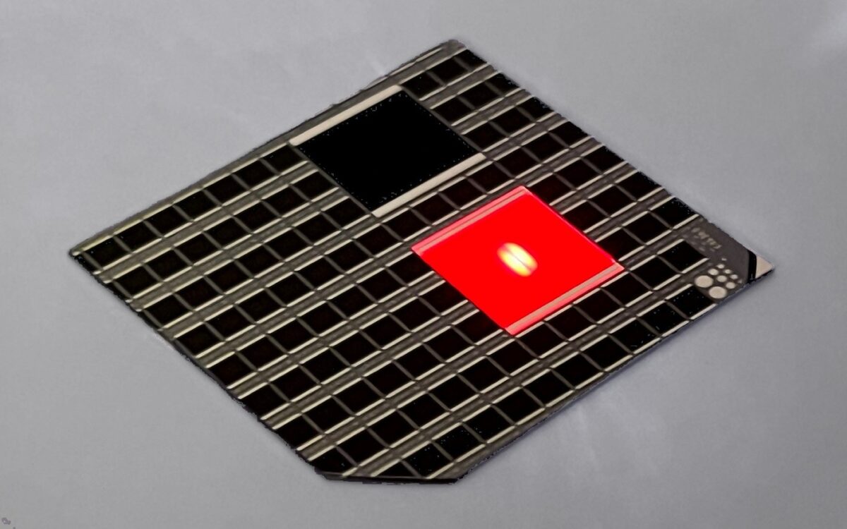
Scientists at the Fraunhofer Institute for Solar Energy Systems ISE (Fraunhofer ISE) in Germany have developed an indoor gallium indium phosphide (GaInP) that achieved a power conversion efficiency of over 40%.
GaInP is a III-V semiconductor material that is commonly utilized in high-power and high-frequency electronics due to its higher electron velocity compared to silicon and gallium arsenide. It has an energy bandgap of 1.9 eV, which the researchers described as “ideal” for indoor applications.
Gallium arsenide (GaAs) and other III-V materials – named after the groups in the periodic table they belong to – are among the best known in terms of efficiency potential for solar cells. Their high production costs, however, have so far limited them to niche applications powering satellites and drones. In these devices, low weight and high efficiency are more pressing concerns than the cost of energy produced.
“We investigated how well the solar cells with different architectures work under low light conditions,” said lead researcher Malte Klitzke. “It was shown that the n-doped GaInP cell performs significantly better than the p-doped cell. N-doped GaInP cells generate more charge carriers and produce more electricity, even under very weak light. This enabled us to achieve very high efficiencies with them in our experiments when converting weak indoor light into usable power.”
In the study “Optimization of GaInP absorber design for indoor photovoltaic conversion efficiency above 40%,” published in Applied Physics Letters, the research team explained that both p-type and n-type GaInP double heterostructure (DH) were grown lattice-matched on gallium arsenide (GaAs) to investigate charge carrier dynamics, with doping being executed through electrochemical capacitance-voltage profiling.
The cells were fabricated with homojunction and rear-heterojunction architectures, with an absorber thickness of 700 nm and 850 nm, respectively, and were processed via photolithography and wet chemical etching. “Ohmic metal contacts were deposited on both wafer sides, with a full-area backside contact and a frontside grid with parallel fingers and a busbar for efficient current collection,” the academics said. “Devices were separated by wet chemical mesa etching, and a two-layer anti-reflection coating was applied.”
The cell was found capable of reaching an efficiency of 37.5% at 100 lx and 40.9% at 1000 lx. “For illumination intensities above 700 lx, the higher-doped rear-heterojunction device exhibited the highest efficiencies, reaching 41.4% at 1000 lx,” the paper notes.
The high efficiency levels were attributed by the research team to the n-type absorber operating under low-light conditions, which they said facilitates the generation of a “significantly larger” number of excess charge carriers. “The rear-heterojunction design maintained higher excess charge carrier densities, leading to superior fill factor and open-circuit voltage compared to the homojunction,” it further explained.
The developed solar cell is intended for use in autonomous Internet of Things (IoT) applications that operate indoors without an external wired power supply.
A recent review of indoor PV cell technologies by an international research team documents over 250 large-area and small-area commercial and laboratory devices. It covers organic, dye-sensitized, and perovskite devices, as well as crystalline and amorphous silicon, III-V semiconductor, chalcogenide, and emerging lead-free alternative cells. The review also includes a discussion about applications, recent progress, and strategies used to design more stable, highly efficient cells that operate at very low light levels.
This content is protected by copyright and may not be reused. If you want to cooperate with us and would like to reuse some of our content, please contact: editors@pv-magazine.com.


By submitting this form you agree to pv magazine using your data for the purposes of publishing your comment.
Your personal data will only be disclosed or otherwise transmitted to third parties for the purposes of spam filtering or if this is necessary for technical maintenance of the website. Any other transfer to third parties will not take place unless this is justified on the basis of applicable data protection regulations or if pv magazine is legally obliged to do so.
You may revoke this consent at any time with effect for the future, in which case your personal data will be deleted immediately. Otherwise, your data will be deleted if pv magazine has processed your request or the purpose of data storage is fulfilled.
Further information on data privacy can be found in our Data Protection Policy.