Scientists at the Nanjing University of Posts and Telecommunications in China have fabricated a kesterite (CZTSSe) solar module prototype that can achieve a power conversion efficiency of 10.1%.
The researchers said the result was certified by the U.S. Department of Energy's National Renewable Energy Laboratory (NREL).
The new module is based on CZTSSe solar cells with an efficiency of 13.4%. The world record for such cells is 14.6%, achieved by the Chinese Academy of Sciences (CAS) in June 2024.
Kesterite is one of the most promising light absorber material candidates for potential use in lower-cost thin-film solar cells. Kesterites include common elements such as copper, tin, zinc, and selenium. Unlike CIGS compounds, there are no supply bottlenecks expected in the future. However, kesterite is still less efficient than CIGS in mass production.
The academics explained that the solution-based fabrication process of thin-film CZTSSe cells involves two critical steps: precursor deposition and high-temperature crystallization. This seemingly clear pathway conceals a significant pitfall that multiphase fusion reactions easily cause compositional inhomogeneity and electronic property fluctuations in the film, becoming a barrier to efficiency enhancement and industrialization of CZTSSe solar cells.
“We have made a breakthrough in achieving direct phase transformation crystallization based on Cu+-Sn4+ solution method, pushing CZTSSe solar cell efficiency to over 13%,” the research's corresponding author, Shaoying Wang, told pv magazine, noting that, however, one of the biggest challenges of their work was to maintain the high efficiency at the module level.
“Initially, the efficiency of our first fabricated CZTSSe module was only 4.3%, with a staggering cell-to-module power conversion efficiency (CTMPCE) loss of 56.81%, which reveals a hard truth that the success of highly efficient small-area cells in the lab is far from equivalent to producing high-quality large-scale absorber films,” he explained. “We further embarked on an in-depth exploration of the large cell-to-module loss.”
Through the characterization and analysis of the film morphology and element distribution during different stage of crystallization process, a key issue emerged: during the early stage of the selenization, a dense crystalline layer already forms on the surface of the film, which acts as an invisible barrier as a hard shell and seriously hinders the subsequent penetration of selenium vapor into the interior of the film.
“This hinders the grain growth in the vertical direction and results in poor film uniformity and high surface roughness,” said Wang. “The nonuniform absorber film cannot support the manufacturing of efficient and large-area devices, accounting for the poor performance and large CTM loss of our previous modules.”
The group decided to change the microstructure of the precursor film used for the perovskite absorber and regulate its porosity to prevent the rapid formation of a dense top layer at the early stage of the selenization and create more space for subsequent selenium (Se) permeation and more time for lateral grain growth, in an effort to improve film uniformity.
The microstructure of the precursor film was closely linked to the composition of the precursor solution, which was based on Thiourea (Tu), a reagent that decomposes during thermal decomposition and releases volatile gases from the film, thus helping increase the film porosity.
“Therefore, we systematically regulate the ratio of Tu to metal ions in precursor solution and investigate the film morphology,” Wang went on to say. “The results were encouraging: after increasing the Tu content, the precursor film became more porous and looser, enabling the formation of a looser top crystalline layer at an early stage of the selenization, which allows more Se to penetrate into the film bulk and provide more room for lateral grain growth and eventually improve the uniformity and surface flatness of CZTSSe absorber film.”
The 0.1 cm2 cell was built with a substrate made of soda lime glass (SLG) and coated with molybdenum (Mo), a CZTSSe absorber, a cadmium sulfide (CdS) layer, a buffer layer made of zinc oxide (ZnO), an indium tin oxide (ITO) layer, and aluminum (Al) and nickel (Ni) metal contacts.

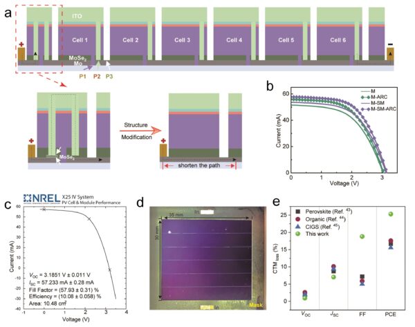
“Based on the improved uniformity of the absorber film, we successfully achieved an average efficiency of 13.4% for single-cells with very low standard deviation and an 8.91% efficiency for the solar module,” Wang stressed. “But this was not the end. We had further modified the module structure to reduce non-ideal contact and shunting caused by series resistance, resulting in a certified 10.1% efficiency and an aperture area of 10.48 cm2 with a low CTMPCE of 25.3% and the lowest CTM loss in open-circuit voltage (0.93%) and short-circuit current (7.03%) among state-of-the-art emerging thin-film solar modules.”
“This is not only the first record efficiency solution-processed CZTSSe module, but also a journey for understanding and tackling the underlying challenges in the fabrication of inorganic thin films via solution approach,” he concluded. “This work provides a clear and feasible technical pathway for solution-processing of high-performance large-area inorganic compound thin-film solar cells and modules.”
The new cell and panel technology was presented in the paper “Solution-processed kesterite solar module with 10.1% certified efficiency,” which was recently published in nature energy.
In April 2023, other researchers at the Nanjing University of Posts and Telecommunications designed a kesterite (CZTSSe) solar cell through a new selenization approach that reportedly ensured the high-crystalline quality of CZTSSe absorbers, with low defects.
This content is protected by copyright and may not be reused. If you want to cooperate with us and would like to reuse some of our content, please contact: editors@pv-magazine.com.


By submitting this form you agree to pv magazine using your data for the purposes of publishing your comment.
Your personal data will only be disclosed or otherwise transmitted to third parties for the purposes of spam filtering or if this is necessary for technical maintenance of the website. Any other transfer to third parties will not take place unless this is justified on the basis of applicable data protection regulations or if pv magazine is legally obliged to do so.
You may revoke this consent at any time with effect for the future, in which case your personal data will be deleted immediately. Otherwise, your data will be deleted if pv magazine has processed your request or the purpose of data storage is fulfilled.
Further information on data privacy can be found in our Data Protection Policy.