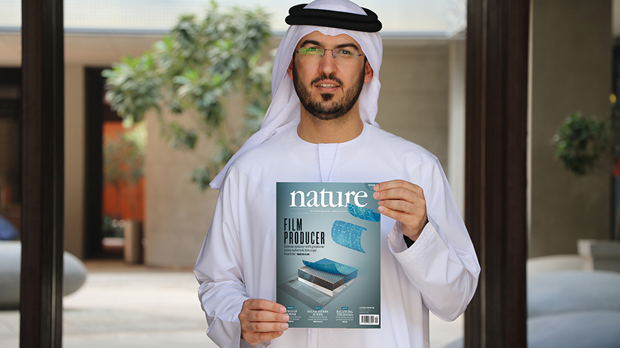
A report published in scientific journal Nature explores the development of a new method for fabricating semiconductor materials. The paper, entitled “Remote epitaxy through graphene enables two-dimensional material based layer transfer” is published as part of a collaboration between Masdar and MIT.
“Having a collaborative project published in nature reflects the quality of the research being undertaken, and the strength of our collaboration with MIT,” says Steve Griffiths, Masdar Institute’s Vice President for Research. “Masdar Institute aims to advance science and engineering in key sectors of relevance to the UAE, and this work is evidence of progress toward that objective.”
The method described in the paper involves growing a thin layer of high bandgap III-V semi-conductor material over a silicon wafer to form a tandem structure. A graphene layer is added to the wafer, allowing new semiconductor layers to grow and easily be peeled off. According to MIT, the process could increase theoretical efficiency limits to more than 43%, and further reduce solar’s LCOE.
III-V materials, have several advantages over silicon as a material for solar cells, however their high cost has meant that so far, they have only been viable for niche projects such as satellites and others where cost is secondary to the need for high efficiency.
“Once it becomes possible to make III-V semiconductors more cost effectively, other people will jump in to improve parts of the process, says Jeehwan Kim, Assistant Professor of Mechanical Engineering at MIT. “With each advance, more uses will open up, especially in solar energy where the cell has clear efficiency advantages.”
This content is protected by copyright and may not be reused. If you want to cooperate with us and would like to reuse some of our content, please contact: editors@pv-magazine.com.


By submitting this form you agree to pv magazine using your data for the purposes of publishing your comment.
Your personal data will only be disclosed or otherwise transmitted to third parties for the purposes of spam filtering or if this is necessary for technical maintenance of the website. Any other transfer to third parties will not take place unless this is justified on the basis of applicable data protection regulations or if pv magazine is legally obliged to do so.
You may revoke this consent at any time with effect for the future, in which case your personal data will be deleted immediately. Otherwise, your data will be deleted if pv magazine has processed your request or the purpose of data storage is fulfilled.
Further information on data privacy can be found in our Data Protection Policy.