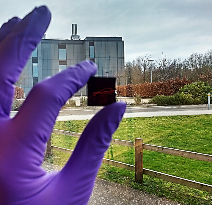
The recent progress in perovskite solar cell efficiencies has been well documented, and the technology seems to have been on the verge of major commercial production for a few years now.
One of the main issues still holding perovskites back, however, is the fragility of the perovskite layer itself. This has often been shown to be sensitive to moisture and other conditions cells are likely to face in the field, and they can also suffer damage as the other layers are deposited on top of it.
The sputtering process commonly used to deposit a transparent electrode layer onto the perovskite is a particular problem here. Several solutions already exist to prevent damage to the perovskite during this process. Scientists at the University of Cambridge, however, have taken a different approach to the issue, which they say will open new possibilities for highly efficient, semi-transparent perovskite devices.
Copper oxide
The group developed a process to ‘print’ a layer of copper oxide onto the perovskite. The layer can be deposited at a low temperature using a technique that does not damage it. And even at only 3 nanometers thick, the copper oxide layer was shown to protect the perovskite from damaging during the sputtering of the transparent conductive oxide. The process is described in the paper Rapid Vapor-Phase Deposition of High-Mobility p-Type Buffer Layers on Perovskite Photovoltaics for Efficient Semitransparent Devices, published in ACS Energy Letters.
“Key to success is the ability of their oxide growth method to replicate the quality of precise, vacuum-based techniques, but in open air and much faster,” reads a statement from the university. “This minimizes any damage to the perovskite while ensuring that the oxide grown has high density, such than only a very thin layer is needed.”
Perovskite solar cells fabricated with this copper oxide layer achieved maximum efficiencies of 16.7%. The semitransparent cells were integrated into tandem devices with silicon cell technologies including p-type PERC and the n-type ‘monoPoly’ cells develop by the Solar Energy Research Institute of Singapore (SERIS). A four-terminal tandem utilizing the SERIS solar cell achieved a maximum efficiency of 24.4%.
Cambridge says that its deposition technique for copper oxide could potentially be scaled up for commercial production, and that its research represents a new approach to silicon/perovskite tandem cell integration, that will also enable the development of other devices requiring high quality protective layers.
*This article was amended on 10/07/2020 to include additional information provided by Cambridge University regarding the type of silicon cell used to achieve the best tandem efficiency.
This content is protected by copyright and may not be reused. If you want to cooperate with us and would like to reuse some of our content, please contact: editors@pv-magazine.com.


By submitting this form you agree to pv magazine using your data for the purposes of publishing your comment.
Your personal data will only be disclosed or otherwise transmitted to third parties for the purposes of spam filtering or if this is necessary for technical maintenance of the website. Any other transfer to third parties will not take place unless this is justified on the basis of applicable data protection regulations or if pv magazine is legally obliged to do so.
You may revoke this consent at any time with effect for the future, in which case your personal data will be deleted immediately. Otherwise, your data will be deleted if pv magazine has processed your request or the purpose of data storage is fulfilled.
Further information on data privacy can be found in our Data Protection Policy.