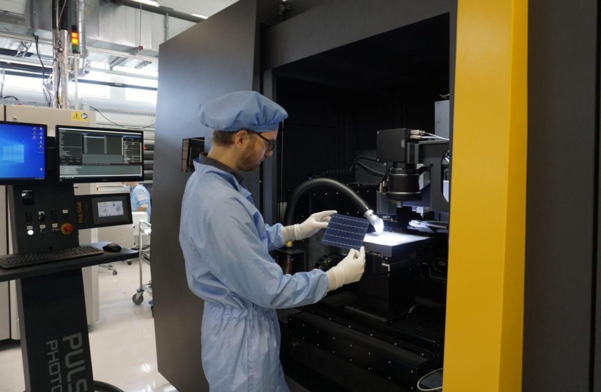
Germany’s Fraunhofer Institute for Solar Energy Systems (ISE) this week unveiled the results of a project exploring alternatives to the screen printing with silver paste currently used to produce the contact fingers on silicon cell surfaces.
The study, backed by Germany’s Federal Ministry of Economic Affairs, also involved laser specialist companies Pulsar Photonics and Soliton, coatings developer ROWO Coating, and PV equipment supplier RENA Technologies.
In silicon solar cell production, screen printing with silver paste is used to apply metal contact fingers to cells to transport electric current out of the devices. The process, however, relies on silver and has limitations on how narrow the fingers can be. Narrower fingers occupy less of the cell surface, raising device efficiency, so more precise manufacturing processes – particularly those which reduce silver content – are of great interest to solar companies.
Alternative processes which have been considered include the plating approach undertaken by the Fraunhofer ISE and its partners.
The institute's ‘laser and transfer firing’ (LTF) process has two steps. First, the cell is placed on a vacuum chuck and moved under a metal-coated foil developed for LTF, with the metal transferred to the cell using direct laser printing. The metal is then formed into a contact using a laser selective-heating process.
The developers of the approach stressed the laser does not damage the silicon material and the process does not heat the cell above room temperature, meaning it can be used for devices with highly temperature-sensitive layers, such as those used in heterojunction cells.
The group claims to have applied metal fingers as narrow as five microns in the lab and said the automated system can be aligned to within a few microns.
The reported goal of the project is to develop an industrial, low-temperature process to manufacture copper contacts for PERC, heterojunction and TOPCon solar cells. Fraunhofer ISE said its process offers materials flexibility and could see nickel replaced with aluminum, titanium or bismuth in future. Moving away from screen printing and achieving very narrow, precise placement also enables the project to experiment with different metallization layouts.
Future plans for a fully ‘layer by layer’ approach to cell metallization could add further flexibility. “In future, in addition to the LTF application, contact fingers are also to be manufactured in their entirety, layer by layer, thus, additively,” said Jan Nekarda, head of structuring and metallization at Fraunhofer ISE. “With the pilot system and our consortium of experts, we hold the best prerequisites to successfully develop these in the future.”
This content is protected by copyright and may not be reused. If you want to cooperate with us and would like to reuse some of our content, please contact: editors@pv-magazine.com.


By submitting this form you agree to pv magazine using your data for the purposes of publishing your comment.
Your personal data will only be disclosed or otherwise transmitted to third parties for the purposes of spam filtering or if this is necessary for technical maintenance of the website. Any other transfer to third parties will not take place unless this is justified on the basis of applicable data protection regulations or if pv magazine is legally obliged to do so.
You may revoke this consent at any time with effect for the future, in which case your personal data will be deleted immediately. Otherwise, your data will be deleted if pv magazine has processed your request or the purpose of data storage is fulfilled.
Further information on data privacy can be found in our Data Protection Policy.