From pv magazine 10/2020
It is often said that Europe is a technological leader, but that its leadership, unfortunately, does not translate into competitive mass production. If Frank Siebke can have his way, that will be about to change. Siebke is the co-founder of NexWafe, a company with a laboratory housing a colossal furnace that produces wafers for silicon solar cells in a way that is completely different from the usual process. The wafers exit the machine looking, in Siebke’s words, “like the rooftops of Gothic cathedrals.” The custom-built machine has been 20 years in the making.
Siebke, who is currently the chief financial officer of NexWafe, has big plans. Next year he intends to start building a 400 MW wafer production facility in Germany, later to be expanded to 3 GW. At the same time, the apparently revolutionary process aims to cut the cost of wafers in half while also slashing silicon consumption and energy requirements. “We can reduce CO2 emissions by 80% even with the German energy mix,” he says.
Siebke has witnessed the disappearance of PV manufacturing from Europe over the years. After working for RWE Schott Solar, he became the CTO and investment director at Good Energies, one of the main investors in Q Cells and REC. He has learned a great deal from that debacle, and now wants to play a role in rebuilding the industry in Europe.
But is NexWafe’s agenda credible? Slashing costs in half while manufacturing in Europe, and at the same time increasing both sustainability and profitability? The secret to success is said to lie in the company’s revolutionary approach.
Epitaxial wafers
Karl Friedrich Haarburger is Nexwafe’s chief operating officer, responsible for managing production. “Our method replaces several steps of conventional wafer production,” he explains. “Here, ingots are pulled and then sawn, a 170 micron wafer produces 70 microns of dust. We replace the processes of polysilicon production, crystallization and sawing with just one other step.”
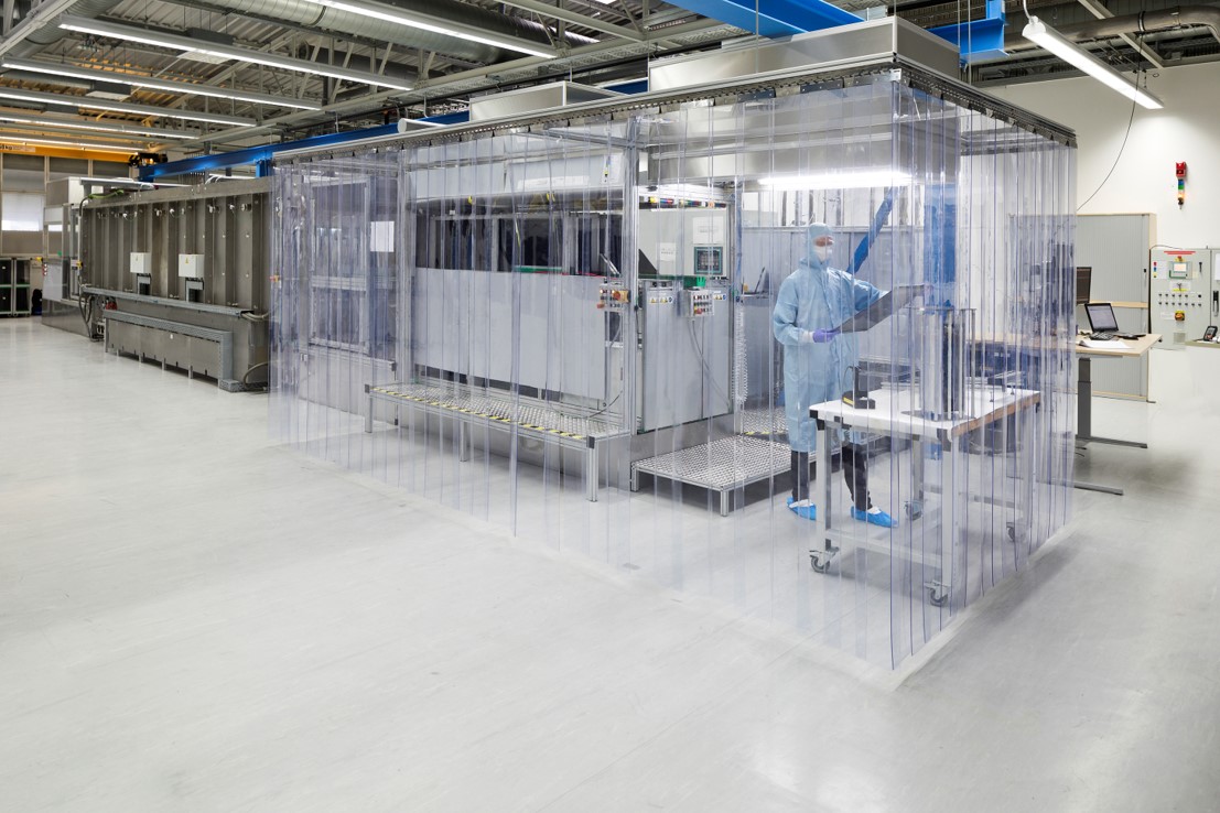
Inside the laboratories at the TDK Micronas site in Freiburg, we get a look at NexWafe’s approach in action. First, monocrystalline seed wafers pass through a bath in which the top layer of the wafer is etched. Then they are fed into the 14-meter-long machine – this is still done by hand on the laboratory line. The machine then heats the wafers. This creates the structure that Siebke describes as “like a Gothic cathedral”: a wafer-thin monocrystalline silicon layer standing on a few nanometer-sized silicon columns on the seed wafer.
These seed wafers then pass through a 1,200 degree Celsius chamber filled with a mixture of hydrogen and chlorosilane. In this so-called epitaxial chamber, crystalline silicon is deposited on the surface of the seed wafer. The result is 50-, 100- or even 170-micron thick monocrystalline wafers, depending on how long they remain in the chamber. Finally, they exit the line in three lanes. One of the lines has already been built as it will be constructed in the factory in two years. Running several individual lanes in parallel will enable a machine of this type to produce wafers 80 microns thick, with a throughput of more than 5,000 pieces per hour.
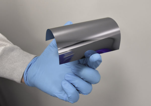
The freshly grown wafers are still fused to the seed wafer. To separate them, the edges are trimmed in other machines and the “epiwafer” – the wafer grown on the seed – is mechanically separated from the seed wafer, which can then be reused about 50 times before it needs to be replaced or reconditioned.
As is so often the case in photovoltaics, this process is not completely unheard-of. Sony filed patents for the process as early as 1997. The Institute for Solar Energy Research Hamelin and Belgium’s imec have also worked on it, says Siebke. But unlike his company, these institutes developed a ‘batch’ process, in which wafers are moved in and out of chambers, taking three hours to produce just twelve wafers. Inline processes, in which wafers pass continuously through the machines, have a much higher throughput. “Fraunhofer ISE started developing this 20 years ago,” says Siebke, who founded NexWafe in 2015 with a group of ISE researchers under the leadership of Stefan Reber. Siebke sees the inline process with its increased speed as the main innovation. The technical details of wafer etching, deposition and separation are understandably not something he likes to discuss publicly.
Siebke has been burned before. One often hears the accusation that German engineers are themselves partly to blame for the decline in German manufacturing, since they first developed expertise in cooperation with the solar cell manufacturers and then sold the systems to China. “We are no longer giving away our know-how,” he says. NexWafe will plan its orders and allocate them to suppliers in such a way that no one will be privy to the entire process and subsequently in a position to resell it. All that will be for sale – preferably on a global scale – will be the actual wafers, which will not reveal the secrets of their production.
Expansion to Bitterfeld
Before this can happen, however, the company has to become competitive. NexWafe secured the former production facilities of PV Crystalox Solar Silicon GmbH in 2018, and announced the start of production in 2019. Siebke is candid about the fact that production was postponed due to delays at a parts supplier, and the laboratory in Freiburg not operating at full capacity due to the Covid-19 lockdown. Thus, the conversion of the pilot line, which will be used to test upscaling, has only just been completed. Currently, the capacity of 1 million wafers a year is high enough that sufficient quantities can be delivered to cell manufacturers for “qualification.” In fact, this capacity will not be fully utilized, since employees use the line primarily to optimize processes.
Construction of the new factory is scheduled to begin next year. Initially, two deposition furnaces based on the design of the plant in the Freiburg lab will be built with a much higher throughput. This should make it possible to produce 400 MW of wafers annually. After that, a further upscaling to 10 systems, and thus 3 GW, is planned. Siebke estimates the investment costs for both steps at €260 million.
Whether they succeed in this will depend in no small measure on whether they think they can convince others of their competitiveness. With large-scale production in the gigawatt range, p-type wafers today account for one-quarter to one-sixth of PV panel costs, at around $0.05/W. The polysilicon accounts for slightly less than half of this amount, and just over half is the cost of producing the single crystal and sawing the wafers. At present, most wafers are produced in Asia, which makes keeping in step with low prices a major challenge.
What the NexWafe model has going for it is the savings it can achieve in silicon. Initially, it will produce wafers 120 microns thick. Compared to standard 170-micron thick wafers, with their losses during sawing, the company already saves half of the energy-intensive silicon. “Even at this stage, we will produce more cheaply,” says Siebke, and 60-micron thick wafers would require just a quarter of the silicon needed for conventional wafers.
The quality, with regard to contamination and uniformity of specific electrical resistance and thickness, is also better than with conventional processes, says Siebke. In addition, higher efficiencies can theoretically be achieved with thinner wafers. Overall, an efficiency boost of more than 2% over standard wafers is possible, according to the experts at NexWafe. Furthermore, p-type and n-type wafers can be produced at the same cost. The method thus makes the most of its advantages when producing thin wafers for n-type high-efficiency cells.
This fits nicely with two other projects in Europe. EcoSolifer has just ramped up a small production facility for n-type heterojunction cells in Csorna, Hungary, and Meyer Burger intends to set up one as well. Siebke sees considerable opportunities for the use of thinner wafers with heterojunction technology. This is because they are metallized equally on the front and back, which he says reduces mechanical stress and the risk of breakage.
Production revolution
When other experts are asked about the concept, they often refer to U.S. company 1366 Technologies, which also makes thin wafers without crystal growth or sawing. However, it can only produce multicrystalline wafers. NexWafe, on the other hand, uses a completely different process to produce the monocrystalline wafers required for high-efficiency cells, and is thus fully aligned to the market trend, unlike 1366.
Nevertheless, analysts have little knowledge of the new processes. Factors such as throughput, expected investment cost and the amount of energy required are not clear, and so they still cannot accurately assess its competitiveness. They also point out that during direct deposition, silicon can be lost due to buildup on the chamber walls, as well as wondering whether the promised homogeneity can really be achieved, how high the wafer breakage rate is, or whether cell manufacturers even want such thin wafers. “One of the challenges in thin wafer production is yield, especially as wafers get bigger, which is why manufacturers have not reduced thickness further,” says Yali Jiang, an analyst at Bloomberg NEF. “But the hurdle is still in cell and module production.” Many of these difficulties can only be properly assessed once you really get into mass production.
In the past, time has always worked against new technologies, as conventional methods have become cheaper and better more quickly than expected. This was what happened with the Recharge Czochralski process, which was used at large scale in ingot production starting in 2018, and the accompanying switch to diamond wire saws which significantly reduced sawing waste. In the market, NexWafe will be competing with players such as Longi, which have production capacities many times greater and have been steadily optimizing costs for years.
So, the challenges are great. Yet it does not look as though manufacturers in Asia are working on similar processes, and NexWafe really has a unique selling proposition. Thus, if Frank Siebke and his colleagues are successful, this innovation could actually lead a renaissance of manufacturing in Germany. “Despite all of the skepticism in view of the lack of information,” says Exawatt analyst Alex Barrows, “I can imagine as a route to market that the resulting products are targeting Western markets for high-efficiency, made in Europe, low materials consumption and a small carbon footprint, for which customers pay a premium.”
One question is whether political measures are needed to support the buildup of production. NexWafe, together with EcoSolifer and SunEdison, is a member of the Genuine Green Europe consortium, which has presented plans to build a 2 GW production facility as part of Solarpower Europe’s Accelerator Initiative and will likely seek support from the EU for at least part of the targeted €1 to €1.2 billion investment.
What Siebke wants above all is a stable framework for the European market. “In the past, I’ve had the impression that some politicians were behaving like new drivers when it came to the energy transition,” he says, “First they rev the engine, and then they stall it out.” He hopes this will not be repeated, and that customers will consider environmental and social standards when selecting products in the future. For example, putting a price tag on CO2 as France does in public tenders could help to build up production capacity. However, he says, this is not necessary for production to begin next year.
This content is protected by copyright and may not be reused. If you want to cooperate with us and would like to reuse some of our content, please contact: editors@pv-magazine.com.

1 comment
By submitting this form you agree to pv magazine using your data for the purposes of publishing your comment.
Your personal data will only be disclosed or otherwise transmitted to third parties for the purposes of spam filtering or if this is necessary for technical maintenance of the website. Any other transfer to third parties will not take place unless this is justified on the basis of applicable data protection regulations or if pv magazine is legally obliged to do so.
You may revoke this consent at any time with effect for the future, in which case your personal data will be deleted immediately. Otherwise, your data will be deleted if pv magazine has processed your request or the purpose of data storage is fulfilled.
Further information on data privacy can be found in our Data Protection Policy.