Scientists at India's SSN College of Engineering have developed a new thermal pyrolysis process to recycle silicon in end-of-life solar panels.
Described in the study Recovering Resources from the End-of-Life PV Modules, published in AIP Conference Proceedings, the new method is claimed to allow the reuse of silicon from the recycled panels in the production of new solar cells.
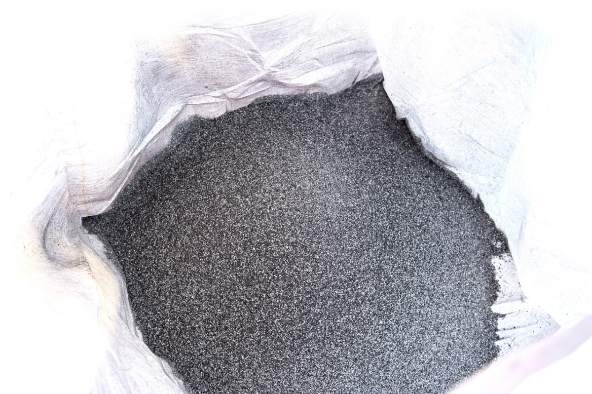
Pyrolysis is the chemical decomposition of organic materials through the application of heat. It is usually carried out at very high temperatures and in the absence of oxygen. “Pyrolysis in a fluidized bed reactor is the best technique for an industrial scale recycling process which contains very fine sand particles which act like a liquid due to high temperature,” the researchers explained. The EVA and back films are evaporated by placing the modules' wafers on a fluidized sand bed.
Compared to other techniques based on chemical reactors and organic solvents, the proposed method is said to be able to maintain a “good mechanical yield” in the recovered solar cells. “Size of the sand particles in the fluidized bed reactor is a main factor to determine the mechanical strength of the silicon solar cell,” the Indian group said. “By optimizing the fluidization velocity of the sand particles, the cells can be harvested safely.”
When pyrolysis is completed, both unbroken and broken wafers go through the chemical etching process to recover the pure silicon wafers from the silicon solar cells. Silver is dissolved through nitric acid (HNO3) and then recovered from the resulting waste acid. The aluminum layer and n or p junctions are also recovered, through different acid solutions. “The yield and purity of the recovered silicon material mainly depend on the concentration of acids and the optimal temperature condition,” the academics stated, adding that the unbroken wafers are reused for the manufacturing of new solar cells and the broken ones are used as a feedstock material for growing new silicon ingots.
According to the research group, the purity and quality of the recycled wafers were ensured by energy dispersive spectrometry (EDS) and minority carrier lifetime measurements.
This content is protected by copyright and may not be reused. If you want to cooperate with us and would like to reuse some of our content, please contact: editors@pv-magazine.com.


I am very happy to know the process of recycling.Dur tothis dumping of used pv panels will be reduced snd some value wiil get for purchasin new panels.Thanks for research teem.
Er Hanmant N Kanihal
Retired CEE KPTCL (2000 NOV)
Propagating since 2010 use of solar energy for Irrigation which will reduce energy losses and economy