While the first commercial perovskite-silicon tandem cells are expected to roll off production lines sometime next year, there’s still plenty more work to be done, both in pushing for higher efficiencies and translating achievements made on small laboratory devices into something that can be replicated and mass produced.
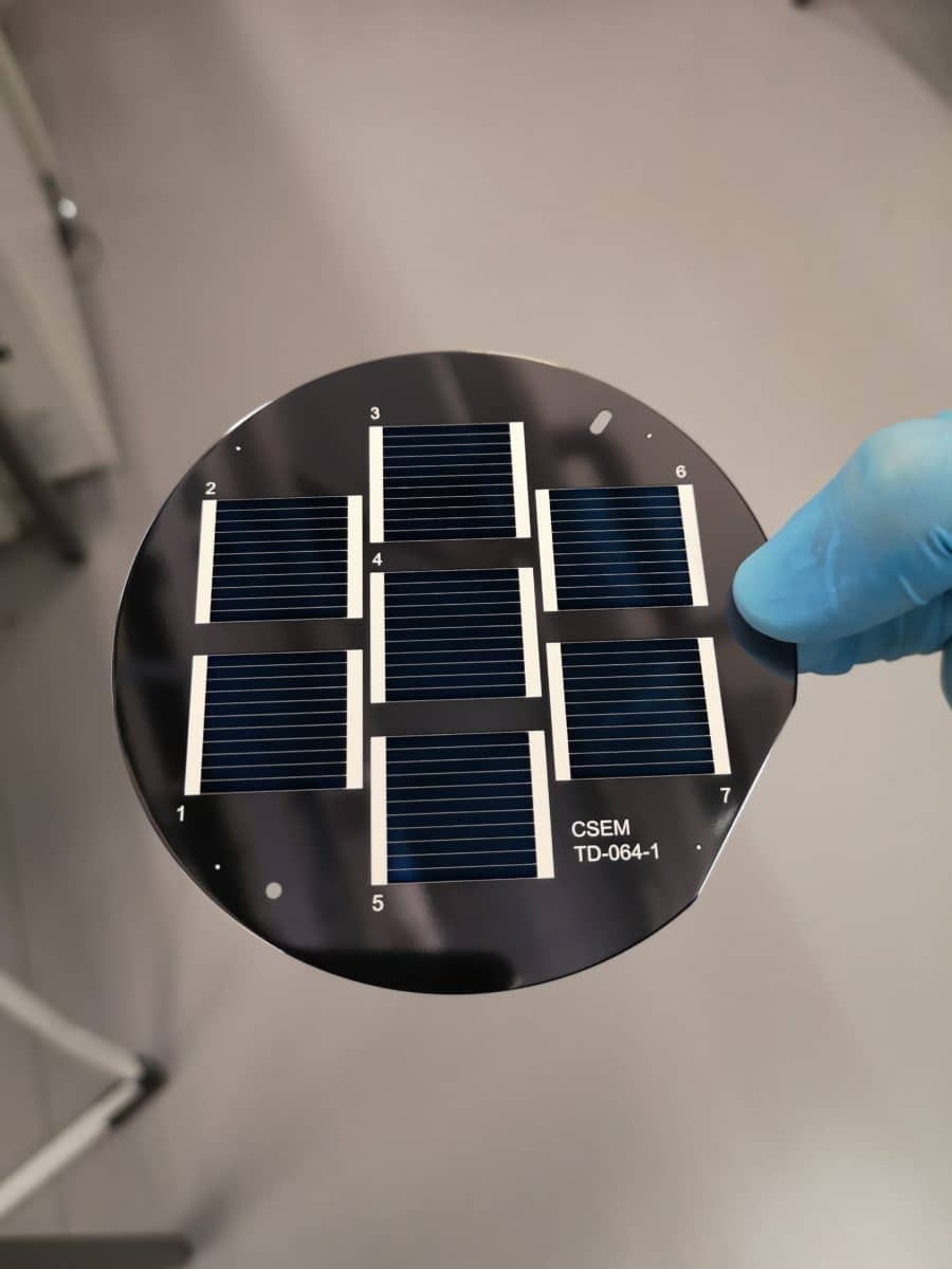
The Swiss Center for Electronics and Microtechnology (CSEM) this week reports progress on both of these fronts, claiming 26.5% efficiency for a tandem device measuring 4cm². The device comprises a single side textured silicon heterojunction (HJT) cell fabricated at CSEM, with a mixed halide perovskite deposited on top.
Though the perovskite layer is deposited using spin coating – a lab process not typically associated with large-scale production, CSEM points out that its cell features screen-printed contacts, while most of the leading tandem cell efficiencies reported have relied on thermally evaporated silver contacts, which would be prohibitively expensive in mass production.
Other than lowering the temperature to 130 degrees Celsius to avoid damage to the perovskite, CSEM says that its screen-printing process is comparable to those used in industrial HJT cell production. And thanks to several improvements, CSEM was able to push the efficiency significantly past the 25.4% it achieved last year, as well as scaling the device up to 4cm2, rather than the more typical research size of 1cm².
Key to the new efficiency, according to CSEM, is its work on the interface between the two cells, where it inserted an organic passivation layer that pushed the device open-circuit voltage to 1.86 V. Improvements to contact resistance between the fingers and the front electrode also helped, pushing the fill factor to 76%.
CSEM measured the cell efficiency in air without encapsulation, but they have not been subject to light soaking, damp heat or other stability tests.
And the Swiss research institute, which is also involved in a consortium looking to bring heterojunction-IBC technology to mass production in Europe, expects to soon be able to push this efficiency past the 27% mark. Strategies it is investigating for this include working with new transparent electrode materials that will perform better than standard indium-tin-oxide, working on light management within the cell, and placing an additional oxide-based microcrystalline contact between the two cell layers.
This content is protected by copyright and may not be reused. If you want to cooperate with us and would like to reuse some of our content, please contact: editors@pv-magazine.com.


By submitting this form you agree to pv magazine using your data for the purposes of publishing your comment.
Your personal data will only be disclosed or otherwise transmitted to third parties for the purposes of spam filtering or if this is necessary for technical maintenance of the website. Any other transfer to third parties will not take place unless this is justified on the basis of applicable data protection regulations or if pv magazine is legally obliged to do so.
You may revoke this consent at any time with effect for the future, in which case your personal data will be deleted immediately. Otherwise, your data will be deleted if pv magazine has processed your request or the purpose of data storage is fulfilled.
Further information on data privacy can be found in our Data Protection Policy.