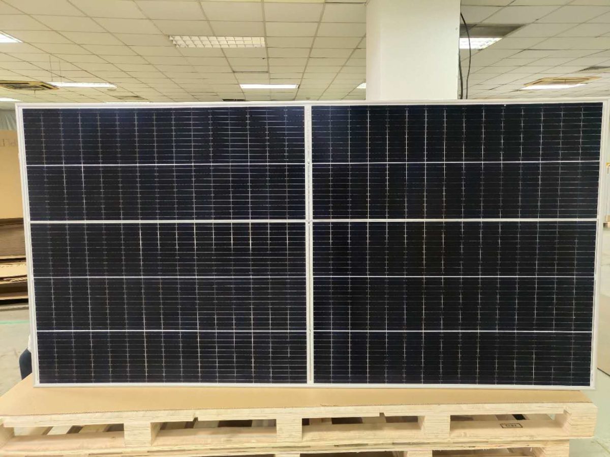
Trina Solar, along with seven other prominent solar module manufacturers, is pushing to standardize 210mm silicon wafers and modules.
The proposal looks to set 210+/-0.25mm as the standard size of silicon wafers in the 210-220mm size range under the Semiconductor Equipment and Materials International Photovoltaic Standards (SEMI), while revising the existing module size standards.
For most of the past decade, the traditional wafer size has been 156.75mm, with that size representing more than 90% of the monocrystalline market. Since 2019 however, manufacturers have begun to see benefits in increasing wafer sizes, leading ultimately to modules rated at 500 W+ appearing on the market.
Because these modules are made by multiple manufacturers, the size change has not been uniform, and that can lead to confusion and increased cost, proponents of the standard said.
Besides setting a standard size, the Trina-led proposal also calls for promoting the standard sizes of silicon wafers and modules as follows:


The companies, which include Risen Energy, Zhonghuan Semiconductor, Tongwei, Huansheng Photovoltaic, Runyang New Energy Technology, Canadian Solar and Wuxi Shangji Automation, alongside Trina, argue that standardizing the silicon wafers will allow the solar industry to achieve scale, and enable all businesses to improve production efficiency, optimize supply chains and drive technological innovation.
The companies also argue that standardization will allow for more competitive manufacturing by decreasing initial investment for new companies and providing some certainty that investments won’t be wasted if a new size becomes more popular.
Trina has been the group’s vocal leader, providing releases supporting the effort, as well as conducting studies to help demonstrate the value and safety of 210mm wafers.
For developers, the companies argue that a 210mm standard will decrease balance of system costs and the levelized cost of electricity for new solar projects.
These balance of system costs refer to large-scale, ground-mount solar projects, the market segment where 210mm wafers are currently practical. With standardization, these larger wafers could be manufactured for smaller-sized modules with a lower power rating. To date, however, they have been utilized in 500W+ modules, which are too large for typical rooftop installations.
Cost savings breakdown
In a company release, Trina outlines why 210mm is the group’s preferred size choice by highlighting flux value, the dumpling effect and cost savings delivered by using fewer modules in an installation. (Fewer modules means lower junction box, potting, combiner box, DC cable, installation and construction costs).
Flux value refers to the increase in production capacity brought about by large-size products, reducing the cost of labor, depreciation, and operating, management and financial expenses per unit of output.
The dumpling effect refers to the increase in the amount of auxiliary materials in transportation, such as frame, glass, backsheet, EVA, ribbon bus bars, pallets and packaging materials being less than the increase in module area when using large-size wafers in module production, bringing savings in encapsulation and transportation costs.
The company also offered a cost calculation of 210mm wafers, compared to 166mm and 182mm wafers, across the entire value chain:

High temps not a concern
In a separate study, Trina addresses one of the most prevalent concerns facing the standardization of 210mm wafer size: the high working temperature of such modules due to their high-current output.
As a module’s operating temperature rises, the open-circuit voltage will decrease, while the short-circuit current increases slightly, leading to decreases in photovoltaic conversion efficiency and cell power. According to the company study, an energy loss of 0.20% occurs for every 1℃ of increase in operating temperature.
The same study, however, found that, under the same installation and cooling conditions, the working temperature of 210mm and 182mm modules are nearly the same. It said that the cells only change the area with the same Passivated Emitter and Rear Cell (PERC) structure and efficiency.
According to Trina, 210mm and 182mm cells have the same PERC structure and their efficiency is almost the same. With similar packing materials and under the same optical environment, there is almost no difference in the current density of such modules. The increase in current in the 210mm ultra-high-power module is driven by a larger cell, as current is the product of current density multiplied by cell area.
And even though the current is larger, efficiency remains the same with a steady current density and larger cell area. In addition, for the same module efficiency, the amount of unutilized heat – the solar energy which cannot be converted into electric energy – is the same in terms of unit area.
With the same installation and heat dissipation conditions, operating temperatures for 210mm ultra-high power modules and 182mm modules are roughly the same, it said.
This content is protected by copyright and may not be reused. If you want to cooperate with us and would like to reuse some of our content, please contact: editors@pv-magazine.com.


This sounds like bs. Start making every obey by their rules and you no longer have competitive increases in technology and slow down growth of effeciency. Product demand should dictate cell size. If people mainly want 210mm for cost savings then they will buy them.
Standardization should help solar be more efficient, lower LCOE and compete with fossil fuels. It should not lead to sub-optimizations or slowed growth.
Preferred cell size will vary per segment, customer etc. Appropriate module size (whether M10 or M12) may also vary with segment (rooftop vs utility), but also module design. Example: back-contact modules are 3-4% smaller with same number/size cells. This is highly relevant to rooftop and other space-constrained segments.