From pv magazine 10/2021
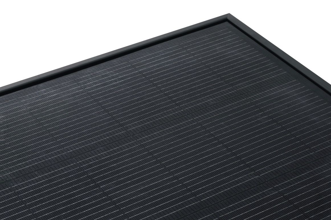
Today, the majority of high-efficiency modules on the market feature half-cut cell designs. Cell cutting was also a key enabler for the ongoing shift toward larger wafer formats – full cell modules based on either 182 mm or 210 mm wafers would be a step backward in terms of performance. And if smaller formats begin to disappear from the market, as many in the industry forecast, cell-cutting processes are likely to become even more ubiquitous in PV manufacturing.
Avoiding damage to the edge of the cell during the cutting process has been a challenge for the industry. Since the largest wafers are often cut into three pieces, and concepts such as shingled cell layouts require even more cutting, and even more cut edges, this can only become more important for the manufacturing industry to address.
Though many manufacturers utilize “scribe and break” processes that can leave damage to the cell edge, equipment suppliers have developed innovative processes to limit this. 3D-Micromac’s thermal laser separation process uses heat from a laser followed by water cooling to create carefully controlled stress that guides a crack through the cell, leaving a clean edge free of microcracks or other damage.
However, this and other “damage free” cell-cutting techniques do still leave behind a new unpassivated area at the edge of the cell, which can lead to performance loss. “In general, cell cutting leads to a minor loss in short circuit current, due to the loss in area, and losses in open circuit voltage and fill factor due to the creation of new unpassivated areas,” explained Shankar Sridhara, CTO at REC Group, which has long used half-cut cells in its Twinpeak modules, and has also integrated them into its latest Alpha heterojunction series.
The loss in open circuit voltage is caused by increased recombination at the unpassivated edge – less of the charge generated can be brought out of the cell and into the module before it is lost. Sridhara goes on to explain that the proportion of open circuit voltage lost increases with the efficiency of the cell, so the challenge will become even more pressing as cell technologies continue to improve.
Heterojunction (HJT) cells, with a highly sensitive amorphous silicon passivation layer, can be at particular risk of performance loss due to cell cutting and loss of passivation. And although REC Group has researched these risks and developed processes allowing it to offer half-cut cells in all of its products, including HJT, new innovations may improve the performance further. “The higher the cell efficiency the greater the loss,” Sridhara said. “Careful process recipes have to be developed to minimize these losses. Additional processes may also need to be developed to passivate the cut edges.”
Edge passivation
Such processes to passivate the cut edges have not yet been seen commercially, but the concept has been proven at the research stage. “Edge recombination cannot be completely prevented, independent of which cell cutting technology is used,” said Thomas Kießling, senior product expert at 3D-Micromac. “However, using edge passivation after cell cutting, it can be significantly reduced, having the highest effects on clean and smooth edges only achieved by thermal laser separation.”
German research institute Fraunhofer ISE has investigated the possibility of post-cutting edge passivation, and developed its “passivated edge technology” (PET), which it describes as a “treatment for separated silicon solar cells consisting of aluminum oxide deposition with subsequent annealing.” Details of this process were first published in 2020, in IEEE Journal of Photovoltaics. In its first round of experiments, Fraunhofer ISE tested the process on PERC cell edges diced into six pieces for shingling, using both 3D-Micromac’s TLS and a mechanical scribe-and-break process. It found that while both cutting processes caused around 1.2% loss in the cells’ pseudo fill factor (pFF), after edge passivation the TLS cut cells saw a pFF increase of up to 0.7%, while the mechanically separated cells were limited to just a 0.3% improvement.
Heterojunction tech
Some manufacturers have been reluctant to integrate cell-cutting processes with heterojunction technology, expecting that the cut will damage the cell passivation layers (which would likely be the case, given that many scribe-and-break processes run at high temperatures). However, further work by Fraunhofer ISE confirms that, with the TLS process at least, performance loss is caused mainly by creation of newly unpassivated edges and not by cell damage or defects. “The temperature of the TLS cleave is far below the melting point of silicon, thus limiting the impact on the hydrogenated amorphous silicon layer,” Kießling pointed out.
Experiments show that heterojunction cells are particularly affected after cutting, but are also great candidates for improvement via edge passivation. While monofacial PERC cells showed a loss in pFF of 0.3% after being cut into shingles via TLS, bifacial HJT cells registered a 2.1% loss in pFF. The group’s most recent work, published in August 2021, shows that at lab scale, edge passivation for HJT half cells, in combination with a light soaking process to activate the aluminum oxide edge passivation layer, brought efficiency of the half cells from 21.7% up to 22.1%, similar to the initial full cell efficiency. Fraunhofer ISE researcher Puzant Baliozian noted that further work is needed to confirm the reason behind the higher losses with HJT cells, and though edge recombination is the main factor, they cannot rule out others related to the cell architecture or its higher initial performance. “But we can say that with the passivated edge technology and a light soaking technique, we have shown an advantage compared to the separation process alone,” he said.
Scaling up
Kießling sees this as clear evidence of the need for damage free cutting processes. “TLS separated shingle stripes regain up to 50% (relative) of their initial pFF loss induced due to separation after PET, with only 16% (relative) regain for scribe and break cut stripes,” he said. “This proves that a smooth edge surface is needed for optimized efficiency gain after edge passivation.” He also noted that similar processes are being investigated elsewhere in the PV research community, pointing to 3D-Micromac’s role in the EU funded Highlite project, where it is aiming to demonstrate high-efficiency shingled cell layouts for HJT and interdigitated back-contact cells.
Fraunhofer ISE’s PET approach is also shown to be appropriate for different cell architectures, including PERC, HJT, and initial results for TOPCon, with fine tuning of process parameters needed for each. Whether a large-scale, cost-effective process can be developed, though, is another matter. Baliozian and colleagues are now working with industrial partners as part of a project titled “Guten Morgen,” to investigate the applicability of large-scale deposition processes, stating that gaining high quality passivation at low temperatures with these larger tools is one upcoming challenge. “This is our next step, to bring it even closer to the industry,” said Baliozian. “But there are some challenges to not give away any quality at all.”
With the direction technology is moving, edge passivation is likely to gain in importance. As for how the process could affect throughput, and ultimately cost, in manufacturing, Baliozian said it is too early to tell, but the potential is there. “How it technically takes place is still under investigation, but we are sure that this topic is of vital importance due to the widespread deployment of cut cells,” he explained. “This becomes even more important with three main factors that are all growing industry trends – the size of the cells, initial output values, and the number of separations.”
Results from edge passivation at laboratory scale are encouraging so far, and the concept has certainly caught the eye of an industry looking to stay ahead of growing challenges. Cell and module makers, as well as equipment suppliers like 3D-Micromac, are already showing an interest. “The long-term goal is to integrate the edge passivation as an additional processing step directly into the TLS tool after cell cutting, we have reserved additional space for that,” said Kießling. “So far edge passivation technology has yet to be commercialized and thus we will have to see what the equipment will look like once it is available for mass production, especially in terms of footprint.”
This content is protected by copyright and may not be reused. If you want to cooperate with us and would like to reuse some of our content, please contact: editors@pv-magazine.com.


1 comment
By submitting this form you agree to pv magazine using your data for the purposes of publishing your comment.
Your personal data will only be disclosed or otherwise transmitted to third parties for the purposes of spam filtering or if this is necessary for technical maintenance of the website. Any other transfer to third parties will not take place unless this is justified on the basis of applicable data protection regulations or if pv magazine is legally obliged to do so.
You may revoke this consent at any time with effect for the future, in which case your personal data will be deleted immediately. Otherwise, your data will be deleted if pv magazine has processed your request or the purpose of data storage is fulfilled.
Further information on data privacy can be found in our Data Protection Policy.