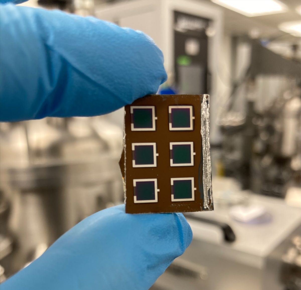
Antimony selenide (Sb2Se3) is a p-type inorganic semiconductor with a one-dimensional crystal structure and a direct bandgap in the range of 1.2 eV to 1.9 eV. It has excellent optoelectronic properties. In recent years, it has also been used as an absorber material to build solar cells. The efficiencies achieved by such devices have reached between 5% and 9.2%.
These efficiency levels are still far behind those of other thin-film technologies, such as cells based on copper, indium, gallium and selenide (CISG), cadmium telluride (CdTe), kesterite (CZTSSe), and amorphous silicon (a-Si). This technological gap might depend on the fact that features such as mobility, carrier lifetime, diffusion length, defect depth, defect density and band tail remain largely unknown to the scientific community for the Sb2Se3 cell technology, as not too many devices of this kind have been fabricated to date.
The latest attempt to investigate such a cell configuration was made by U.S. scientists from the University of Toledo. They developed a device with a power conversion efficiency of 8.5%.
“The efficiency was measured in our own lab so it is internally certified,” researcher Suman Rijal told pv magazine. “These cells can be used for the production of solar electricity and also can be used as a photocathode for the production of hydrogen by the solar water splitting method.”
The cell was built with a two-step closed space sublimation (CSS), which is a physical vapor deposition method to produce thin films. It involves semiconductors that evaporate below 800 C, which are coated on substrates in both vacuum and atmospheric pressure.
“This is a kind of sublimation deposition method this can go for commercial production,” Rijal said.
The scientists applied a seed layer was to a soda-lime glass substrate coated with molybdenum (Mo) through rapid thermal evaporation (RTE). They said this enabled templated growth of a vertically orientated Sb2Se3 seed layer that, in turn, enabled the growth of a high-quality Sb2Se3 absorber layer with high crystallinity and large columnar grains, while also avoiding the void formation at the back interface.
“The seed layer plays a crucial role in controlling the crystalline quality and preferred orientation of Sb2Se3 thin films and their interface properties,” the scientists said, noting that the growth of the Sb2Se3 ribbons can be oriented in mainly two groups of directions with respect to the substrate surface, and that vertically oriented ribbons are preferred.
A cell developed with this configuration originally achieved an efficiency of 7.47%, an open-circuit voltage of 459 mV, a short-circuit current of 26.54 mA cm2 and a fill factor of 61.39%. After post-deposition annealing in the air was used to passivate bulk defects in the Sb2Se3 absorber, the device reached 8.5%.
“The air annealing effectively reduces the densities of the defects and lowers their activation energies,” the scientists said. They also claimed that their research shows that high-performance Sb2Se3 solar cells can be developed through an approach that they define as “facile and effective.”
They shared the technical details of the cell in “Templated Growth and Passivation of Vertically Oriented Antimony Selenide Thin Films for High-Efficiency Solar Cells in Substrate Configuration,” which was recently published in Advanced Functional Materials.
This content is protected by copyright and may not be reused. If you want to cooperate with us and would like to reuse some of our content, please contact: editors@pv-magazine.com.


2 comments
By submitting this form you agree to pv magazine using your data for the purposes of publishing your comment.
Your personal data will only be disclosed or otherwise transmitted to third parties for the purposes of spam filtering or if this is necessary for technical maintenance of the website. Any other transfer to third parties will not take place unless this is justified on the basis of applicable data protection regulations or if pv magazine is legally obliged to do so.
You may revoke this consent at any time with effect for the future, in which case your personal data will be deleted immediately. Otherwise, your data will be deleted if pv magazine has processed your request or the purpose of data storage is fulfilled.
Further information on data privacy can be found in our Data Protection Policy.