Fraunhofer ISE, AMOLF claim record efficiency of 36.1% for silicon-based multijunction solar cell


Germany’s Fraunhofer Institute for Solar Energy Systems (Fraunhofer ISE) and Dutch research institute AMOLF announced they have achieved a world record power conversion efficiency of 36.1% for a multijunction solar cell based on silicon and III-V semiconductors such as gallium indium phosphide (GaInP) and gallium arsenide (GaAs).
“The Fraunhofer team is world-renowned for the fabrication of ultra-high efficiency solar cells based on silicon and III-V semiconductors such as GaInP or GaAs,” the Fraunhofer ISE said in a statement. “The AMOLF team has built up many years of experience in optimizing the management of light in solar cells. In this project, we brought this knowledge together, with this unique result. The solar cells have traveled between Freiburg and Amsterdam for the different processing steps, in this way building up the full solar cell.”
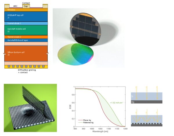
The cell is based on a TOPCon technology developed by the Fraunhofer ISE and a specially designed metal/polymer nanocoating provided by AMOLF. The latter is placed at the silicon sub-cell bottom and is reportedly responsible for optimizing the distribution of light scattering beyond the total internal reflection critical angle in the cell.
“Specifically, we optimize the geometry of a hexagonal array of silver (Ag) nano-disks that are integrated with the Ag back contact, and show how pitch, radius, and height of the individual scatterers control the distribution of power over different diffraction orders, while at the same time minimizing plasmonic dissipation losses in the wavelength range of interest,” the scientists explained.
They also used substrate conformal imprint lithography (SCIL), an innovative full-wafer scale nanoimprint technology, to fabricate the nanopatterned metagrating back-reflectors.
They then connected the top and bottom cells by direct wafer bonding at room temperature. The resulting solar cell has a size of 2 cm x 2 cm and includes front contacts, an anti-reflection coating (ARC), and a 1 μm thick Ag layer on the back side acting as an electrical contact and planar mirror. “After nanoimprint and etching the cells were shipped again to Fraunhofer ISE for a final HF dip followed by metallization,” they explained.
Through several numerical and experimental assessments, the Dutch-German group found that the multijunction device’s external quantum efficiency (EQE) over a planar back-reflector improved by over 1.52 mA/cm 2.
“Overall, our work demonstrates the potential of nanophotonic light trapping for enhancing the efficiency of silicon-based multi-junction solar cells, paving the way for more efficient and sustainable solar energy technologies,” it stated.

Please login to comment
[…] 详情参考 […]
[…] ogniwa, do czego wykorzystano bezpośrednie łączenie płytek w temperaturze pokojowej. Uzyskane ogniwo słoneczne ma wymiary wynoszące 2 cm x 2 cm i zawiera przednie styki, powłokę przeciwodblaskową, warstwę Ag o […]
Great developments , thanks for those working to the better being of their kind
[…] fifth result added to the tables is the 36.1% efficiency that Germany’s Fraunhofer Institute for Solar Energy Systems (Fraunhofer ISE) and Dutch […]