With the EU PVSEC trade conference just around the corner we can expect to see plenty of new cell efficiency records and technology breakthroughs from Europe’s solar focused research institutes in the next few weeks.
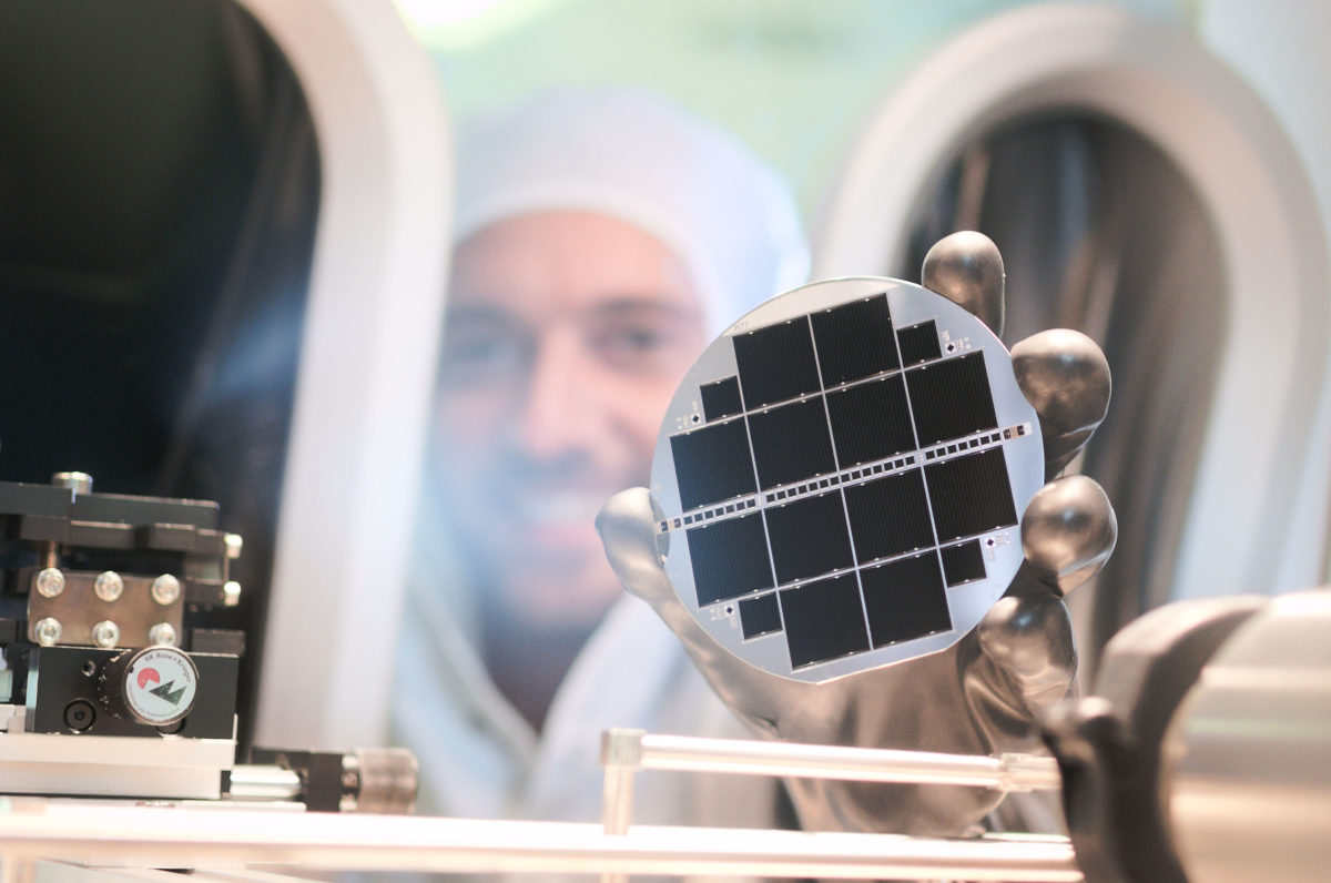
Germany’s Fraunhofer ISE has got in first, setting two records for high-efficiency cell concepts, both using multiple junctions with cells made from III-V materials layered on crystalline silicon.
“Monolithic multi-junction solar cells are a source of hope for the further development of the silicon solar cells dominating the field today because they can lead to significantly higher efficiency values when converting sunlight into electrical power,” wrote institute director Andreas Bett. “We believe that we can achieve efficiency values of 36%.”
Triple junction
Both record-setting devices used three active layers tuned to absorb different ranges of the light spectrum – a top layer of gallium indium phosphide (GaInP) to absorb visible light in the 300-660 nanometer range, an aluminum gallium arsenide (GaAs) layer tuned to near infrared light in the range of 600-840 nm, and a silicon cell absorbing lower wavelength light up to a 1200nm range.
The institute achieved 34.1% efficiency using a process called direct wafer bonding, where the III-V layers are first deposited on a GaAs substrate and then pressed together. The III-V layers bond with the silicon to form a single unit and the substrate is removed in a wet chemical process.
Fraunhofer ISE had also set the previous record for the technology, at 33.3%. Frank Dimroth, head of department III-V photovoltaics and concentrator technology at Fraunhofer ISE, said a new cell structure for the GaInP layer, as well as improvements to the deposition process, were the key innovations that enabled researchers to raise the efficiency.
Cost too high
While an impressive result for the institute, the need for a GaAs substrate and other costly technologies in the process would make it too expensive for mass production. Fraunhofer’s other new record, however, includes fewer process steps and lower production costs – by simply depositing the III-V layers directly onto the silicon cell.
Having first introduced a process for this in December – and achieving efficiency of 22.3% – the institute said it made strong progress in controlling the atomic structure of the III-V layers during their growth and limiting the presence of defects, and has now raised efficiency to 24.3%. And that is just the start, said the institute.
“The potential is comparable to that of the wafer-bonded cells,” said Dimroth. “We’ve got our work cut out for us in the coming years in order to prove that this is the case.”
The institute acknowledged challenges remain to developing a cost-effective process for production of the cells, and said it sees direct growth on silicon as the most promising pathway. Other research institutes, including the National Renewable Energy Laboratory in the United States, have focused on the more expensive bonding process, seeking ways to make the substrate reusable to bring down production costs.
“For cost-effective solar cell production, new deposition machines with [an] higher throughput and deposition area will be required,” read a statement from the Fraunhofer ISE. “These are all methods that researchers at ISE will pursue in the coming years.”
This content is protected by copyright and may not be reused. If you want to cooperate with us and would like to reuse some of our content, please contact: editors@pv-magazine.com.


17 comments
By submitting this form you agree to pv magazine using your data for the purposes of publishing your comment.
Your personal data will only be disclosed or otherwise transmitted to third parties for the purposes of spam filtering or if this is necessary for technical maintenance of the website. Any other transfer to third parties will not take place unless this is justified on the basis of applicable data protection regulations or if pv magazine is legally obliged to do so.
You may revoke this consent at any time with effect for the future, in which case your personal data will be deleted immediately. Otherwise, your data will be deleted if pv magazine has processed your request or the purpose of data storage is fulfilled.
Further information on data privacy can be found in our Data Protection Policy.