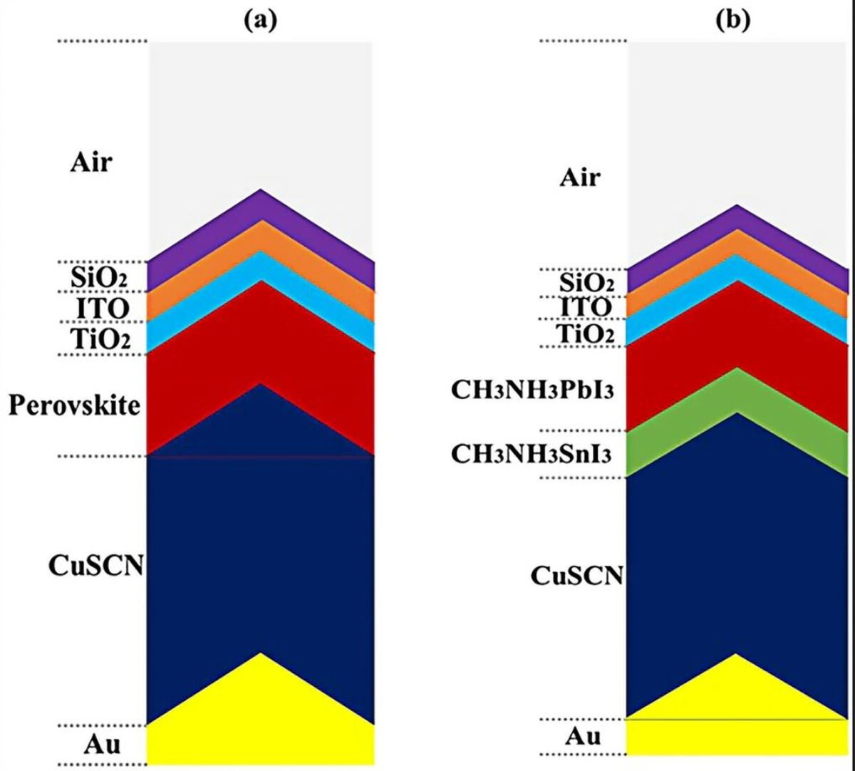
Researchers at the Tarbiat Modares University (TMU) in Iran have designed a two-dimensional perovskite solar cell with a light-trapping (LT) structure and an anti-reflector layer based on silicon dioxide (SiO2).
They said that the combination of these two elements helps to trap light in the whole cell structure, thus offering a significant advantage compared to perovskite PV devices based on a planar structure. “In order to form the described light-trapping structure, the layers of this cell must be placed on a textured silicon substrate,” the scientists explained. “Contrary to planar structures, this structured solar cell should be constructed starting from the bottom layer.”
In solar cells built with an LT architecture, the main issue is the thickness of the absorber, which must be increased compared to that of planar cells in order to achieve higher light absorption. An increased absorber, however, may have negative effects on the electrical properties of the cell itself.
The research group designed the cell by placing the anti-reflective SiO2 layer on the indium tin oxide (ITO) layer and considered the use an absorber made of CH3NH3SnI3, a perovskite material with an energy bandgap of 1.3 eV. It utilized an electron transport layer made of titanium oxide (TiO2), a hole transport layer based on copper thiocyanate (CuSCN) and a gold (Au) metal contact.
Through a series of simulations, the academics compared the performance of the proposed solar cell design with that of a similar cell with a planar configuration. They found that, the reflectance of the LT architecture was lower than that of the planar configuration. “This means that light easily enters the active layer and is confined inside the active layer,” they explained. “Also, because light is difficult to exit, the volume of light entering the active layer increases as the wavelength increases.”
Popular content
The simulation also showed that the most efficient cell designed with LT structure may achieve an efficiency of 20.48%, an open-circuit voltage of 0.96 V, a short-circuit current density of 22.22 mA/cm2 and a fill factor of 83.33%. This cell would require a perovskite absorber with a thickness of 300 nm.
“When the perovskite layer becomes thicker, so does the efficiency of the perovskite solar cell,” they explained. “However, the efficiency practically achieves its maximum when the thickness approaches 200 nm. Thereafter, the efficiency marginally declines.”
They presented the novel cell design in the paper “Design of optimized photonic-structure and analysis of adding a SiO2 layer on the parallel CH3NH3PbI3/CH3NH3SnI3 perovskite solar cells,” published in scientific reports.
This content is protected by copyright and may not be reused. If you want to cooperate with us and would like to reuse some of our content, please contact: editors@pv-magazine.com.


By submitting this form you agree to pv magazine using your data for the purposes of publishing your comment.
Your personal data will only be disclosed or otherwise transmitted to third parties for the purposes of spam filtering or if this is necessary for technical maintenance of the website. Any other transfer to third parties will not take place unless this is justified on the basis of applicable data protection regulations or if pv magazine is legally obliged to do so.
You may revoke this consent at any time with effect for the future, in which case your personal data will be deleted immediately. Otherwise, your data will be deleted if pv magazine has processed your request or the purpose of data storage is fulfilled.
Further information on data privacy can be found in our Data Protection Policy.