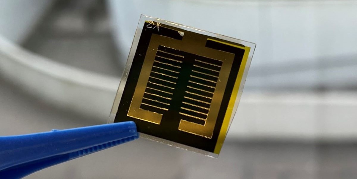
A research team from Karlsruhe Institute of Technology (KIT) has developed a scalable two-step process for organic perovskite thin-film formation that has the potential to be used on textured substrates.
The process, which is described as a scalable and reliable technique for high-quality perovskite deposition, combines the use of an evaporated lead iodide layer with inkjet-printed organic perovskite precursor materials
“It was a challenge and a big success to lift the performance of solar cells based on evaporated lead iodide to the same performance levels of devices with spin-coated lead iodide scaffold,” corresponding lead author, Raphael Pesch, told pv magazine, adding that the team was able to tailor porosity with an inexpensive dimethyl sulfoxide (DMSO) vapor treatment. “We identified early on that the porosity of the lead iodide in the first step is crucial for the conversion in our two-step fabrication process.”
The process is also said to exhibit high reproducibility and potential for conformal growth on textured silicon, and that provide films that are free of drying effects and toxic solvents.
With the proposed technique, the films are deposited using a Pixdro LP50 inkjet printer from German supplier SÜSS, equipped with a Sapphire QS-256/10 AAA print head, which has 16 times more nozzles than typical print heads used in labs for this type of application. “This not only helps increase the droplet-surface interaction time, which is necessary to prevent large-area drying effects but also reduces the probability of pinholes,” said Pesch.
Referring to the Sapphire print head used in the study, KIT's next-generation PV group leader, Ulrich W. Paetzold, pointed out it can also be used in larger printers, such as the n.jet lab from Notion Systems, capable of printing areas of 0.61 x 0.61 square meters at a speed of 2 meters per second.
Paetzold underscored the cost-effectiveness of the process. “The organic precursor materials required for constructing perovskite solar cells can be quite expensive,” he added. “While the material yield tends to be low when evaporated, inkjet printing enables us to achieve a near-perfect material yield of almost 100%.”
Popular content
By optimizing the printing parameters, the group achieved champion devices with an efficiency 18.2%, which it noted is “on par with spin-coated counterparts”.
“We were very surprised in the lab to see the significant impact this additional step has on the cells' performance,” Paetzold told pv magazine, pointing out there is still some work to do to outperform the lab-based spin-coating process.
“The spin-coated reference devices are still slightly better in performance compared to the scalable processes,” said Paetzold. The optimal results in this study were attributed to the morphology of the lead iodide thin film and the selected resolution of the printing process, as well as the intermixing and stoichiometry step enabled by the DMSO vapor treatment to increase the lead iodide porosity.
The novel technique was described in the paper “Hybrid Two-Step Inkjet-Printed Perovskite Solar Cells,” which was recently published in RRL Solar.
Looking ahead, the team will be working on integrating the process into the fabrication of tandem devices and large area devices. “The ultimate goal is to process full-size wafer silicon bottom cells,” said Paetzold.
This content is protected by copyright and may not be reused. If you want to cooperate with us and would like to reuse some of our content, please contact: editors@pv-magazine.com.

By submitting this form you agree to pv magazine using your data for the purposes of publishing your comment.
Your personal data will only be disclosed or otherwise transmitted to third parties for the purposes of spam filtering or if this is necessary for technical maintenance of the website. Any other transfer to third parties will not take place unless this is justified on the basis of applicable data protection regulations or if pv magazine is legally obliged to do so.
You may revoke this consent at any time with effect for the future, in which case your personal data will be deleted immediately. Otherwise, your data will be deleted if pv magazine has processed your request or the purpose of data storage is fulfilled.
Further information on data privacy can be found in our Data Protection Policy.