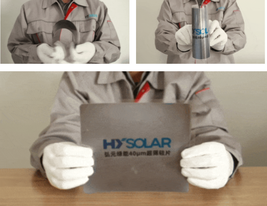
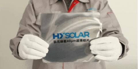
Hongyuan Green Energy said it has produced a first batch of 40 µm ultra-thin monocrystalline silicon wafers at its smart wafer manufacturing base in Baotou, China, marking what it describes as a production-oriented step in wafer thinning rather than a record-setting demonstration. The company dates the milestone to Jan. 23, 2026.
In an official disclosure, Hongyuan said the wafers are compatible with both full-wafer and half-cut processing and cover full-size formats used in mainstream cell and module manufacturing. The “high-precision” slicing step was completed using Hongyuan’s self-developed wafering equipment, which the company said was designed to operate stably at very low thickness.
Hongyuan attributed the result to a series of equipment and process adjustments aimed at controlling stress and breakage during cutting. These include a compact axis-spacing design, ultra-low adjustable tension to stabilise the wire web at higher speeds, and fine-wire, narrow-groove approaches intended to reduce kerf losses. The company also cited dynamic tension control, optimised wire-path design and low-stress cutting to limit vibration- and stress-induced microcracks, alongside online monitoring and feedback linked to a process database.
On material quality, Hongyuan said the wafers feature controlled oxygen and carbon levels, high minority-carrier lifetime and strong resistivity uniformity. It added that its wafer portfolio has passed France’s ECS carbon footprint certification.
Thin-wafer development was a prominent industry focus between 2020 and 2023, when elevated polysilicon prices pushed suppliers and equipment makers to reduce silicon consumption while managing rising breakage and handling risks. During that period, Gaoce (Qingdao Gaoce) showcased 80 µm and later 60 µm half-wafer samples on 210 mm formats and said it had achieved 110 µm half-wafer mass-production capability. Separate industry disclosures linked to Gaoce indicated some customers had received 90 µm deliveries, with 60 µm mass-production pathways under development for heterojunction-related applications.
Among larger incumbents, TCL Zhonghuan has referenced wafer thinning in investor communications, citing 100 µm mass-production capability as part of its cost-reduction strategy. Longi has highlighted ongoing silicon wafer platform upgrades under its TaiRay branding as it reshapes capacity, but has not publicly linked those disclosures to a 40 µm manufacturing target.
This content is protected by copyright and may not be reused. If you want to cooperate with us and would like to reuse some of our content, please contact: editors@pv-magazine.com.

By submitting this form you agree to pv magazine using your data for the purposes of publishing your comment.
Your personal data will only be disclosed or otherwise transmitted to third parties for the purposes of spam filtering or if this is necessary for technical maintenance of the website. Any other transfer to third parties will not take place unless this is justified on the basis of applicable data protection regulations or if pv magazine is legally obliged to do so.
You may revoke this consent at any time with effect for the future, in which case your personal data will be deleted immediately. Otherwise, your data will be deleted if pv magazine has processed your request or the purpose of data storage is fulfilled.
Further information on data privacy can be found in our Data Protection Policy.