Researchers at Panjab University in India have demonstrated a new method for doping silicon solar cells using ion beam technology, achieving improved electronic properties and reduced defect-related losses.
“Defects in TOPCon and PERC solar cells often arise from conventional fabrication processes such as thermal diffusion, radio frequency (RF) sputtering, and plasma-based techniques, where limited control over dopant concentration leads to non-uniform p–n junction formation,” corresponding author Monika Verma told pv magazine. “These established methods can introduce lattice deformation, uneven dopant profiles, and defect complexes, which degrade carrier lifetime and limit charge transport, ultimately reducing efficiency.”
Ion beam implantation offers a route to mitigate these issues by enabling precise control over dopant depth and concentration, reducing impurity-related defects, and improving carrier transport properties. It also supports advanced device architectures through uniform and repeatable junction formation.
The technique involves directing high-energy ions into a material to modify its composition and structure at the atomic level. It is widely used in semiconductor manufacturing to implant dopants, enabling controlled formation of p–n junctions with minimal defects and improved electronic performance.
“Ion beam technology has long been used in the integrated circuit industry and is now re-emerging as a promising tool for photovoltaic applications,” said co-author Sanjeev Gautam. “It offers precise control over dopant concentration, uniform ion distribution, and tunable junction depth based on ion energy and fluence, improving reproducibility.”

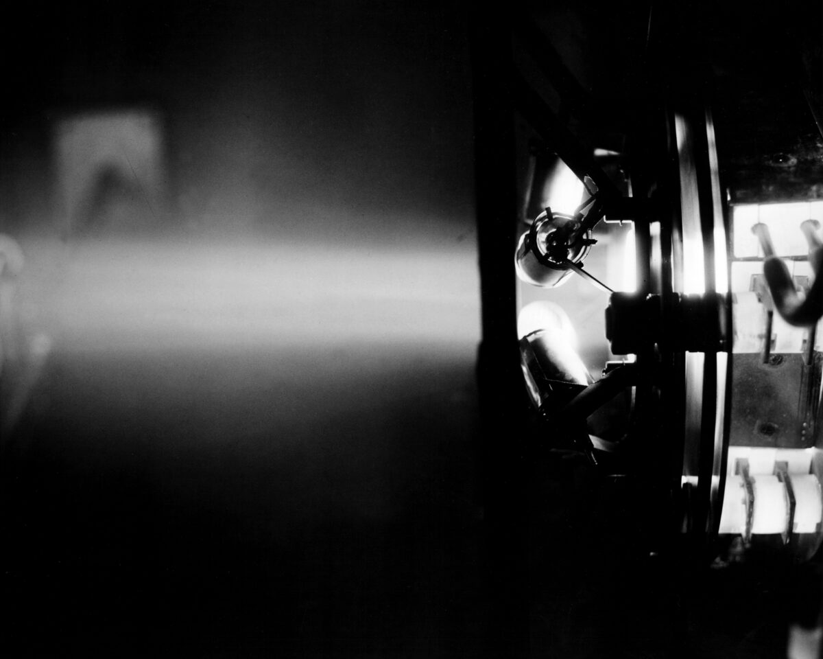
Image: Panjab University
The researchers fabricated a p–n junction by implanting boron ions into n-type silicon wafers at an energy of 35 keV. Compared to conventional thermal or plasma-based methods, the ion beam approach allows highly controlled dopant placement while minimizing structural damage.
They confirmed boron incorporation using X-ray photoelectron spectroscopy (XPS), observing a measurable shift in silicon binding energy. According to the study, XPS showed higher sensitivity than traditional techniques such as X-ray diffraction (XRD) and Rutherford backscattering spectrometry (RBS) for detecting implanted dopants. Additional analysis using near-edge X-ray absorption fine structure (NEXAFS) spectroscopy revealed changes in the local electronic structure consistent with boron integration into the silicon lattice.
“Boron implantation into n-type Si(100) creates a p-type layer, forming the p–n junction,” said Verma. “Measuring dopant concentration is challenging, as many conventional techniques fail to detect low levels. XPS enables direct probing of the chemical environment at the junction, providing dopant detection at parts-per-million levels and confirming boron incorporation through core-level binding energy shifts.”
Electrical testing revealed diode-like current–voltage characteristics consistent with the Shockley model, confirming the formation of a functional p–n junction. The devices exhibited a low leakage current of around 0.63 mA, indicating reduced recombination losses and improved charge transport.
The researchers attributed these improvements to minimized lattice defects, a key limitation in standard silicon solar cell manufacturing. Such defects typically act as recombination centers, reducing carrier lifetime and overall efficiency.
“With this work, we demonstrate how ion implantation can be used to fabricate p–n junctions under controlled conditions,” said Gautam. “Dopants are introduced into Si(100) at defined energy and fluence, forming a thin layer on the nanometer scale. The goal is to minimize crystal damage, much of which can be recovered after implantation, offering a pathway toward next-generation high-efficiency silicon solar cells.”
The novel approach was presented in “Precise dopant detection and transport properties of boron ion-implanted silicon solar cells,” published in RSC Advances.
This content is protected by copyright and may not be reused. If you want to cooperate with us and would like to reuse some of our content, please contact: editors@pv-magazine.com.


By submitting this form you agree to pv magazine using your data for the purposes of publishing your comment.
Your personal data will only be disclosed or otherwise transmitted to third parties for the purposes of spam filtering or if this is necessary for technical maintenance of the website. Any other transfer to third parties will not take place unless this is justified on the basis of applicable data protection regulations or if pv magazine is legally obliged to do so.
You may revoke this consent at any time with effect for the future, in which case your personal data will be deleted immediately. Otherwise, your data will be deleted if pv magazine has processed your request or the purpose of data storage is fulfilled.
Further information on data privacy can be found in our Data Protection Policy.