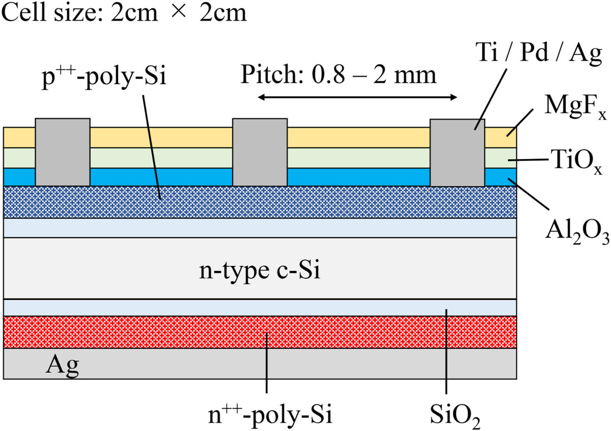
Researchers from the Tokyo Institute of Technology in Japan and Germany's Fraunhofer Institute for Solar Energy Systems (Fraunhofer ISE) have fabricated a solar cell based on n-type tunnel oxide passivated contact (TOPcon) technology by applying a manufacturing technique known as a plasma immersion ion implantation (PIII) or pulsed-plasma doping (pulsed PIII).
The latter consists of a technique for surface modification that, unlike conventional ion implantation techniques, surrounds the targeted element with plasma and pulse biased to high negative voltages. Its advantage lies in the ability to implant the targets with complex three-dimensional geometries, which avoids scanning systems or target manipulators.
In TOPCon PV cells, ion implantation is used to locally overcompensate an in-situ boron-doped TOPCon layer with phosphorus, which improves the cell's electrical and surface passivation quality.
“Ion implantation using PIII system simplifies equipment design and significantly reduces equipment costs by eliminating the number of mass separation systems, acceleration components, large vacuum pumps, and operating stages required for scanning implantation,” the scientists explained. “In addition, throughput can be dramatically increased because PIII system has a large-area ion extraction electrodes that can be used for large-area implantation.”
They built the cell with a 156 mm × 156 mm Czochralski (CZ) n-type wafer with a thickness of 180 μm. They used two different implantation systems known as Beam line system and PIII system for ion implantation and deposited a silicon dioxide (SiO2) layer on both sides by low-pressure chemical vapor deposition (LPCVD). “For the boron doping, BF + ions were used in the beam line implantation system and BF3 plasma was used in the PIII system,” they explained.

Image: Tokyo Institute of Technology, Solar Energy Materials and Solar Cells, Creative Commons License CC BY 4.0
The manufacturing process concludes with a hydrogenation step, which includes the deposition of a 75-nm-thick hydrogenated silicon nitride (SiNx:H) layer on both sides of the cell.
To evaluate the passivation quality of the device, the research group used the quasi-steady-state photoconductance (QSSPC) measurement method, which is a standard tool utilized in silicon-based photovoltaics for injection-dependent measurements of the carrier lifetime of silicon wafers.
The analysis showed that both ion implantation systems used in the experiment achieved almost the same surface passivation quality under optimized conditions, while exhibiting similar short-circuit current and fill factor. It also showed, however, that the Beam line system may result in higher surface passivation quality, which the researchers said could be probably due to the non-optimized annealing conditions.
Tested under standard illumination conditions, the cell fabricated via the Beam line system achieved a power conversion efficiency of 20.5% and the one built via the PII system reached 20.1%. “These results clearly demonstrated that the PIII system can be applied to the production of n-type wafer-based tunnel oxide passivated contact solar cells,” the academics said, noting that this system still has an (iron) Fe contamination problem that should be solved to bring the proposed technique to commercial production.
Their findings were presented in the study “Plasma immersion ion implantation for tunnel oxide passivated contact in silicon solar cell,” published in Solar Cell Materials and Solar Cells.
This content is protected by copyright and may not be reused. If you want to cooperate with us and would like to reuse some of our content, please contact: editors@pv-magazine.com.


By submitting this form you agree to pv magazine using your data for the purposes of publishing your comment.
Your personal data will only be disclosed or otherwise transmitted to third parties for the purposes of spam filtering or if this is necessary for technical maintenance of the website. Any other transfer to third parties will not take place unless this is justified on the basis of applicable data protection regulations or if pv magazine is legally obliged to do so.
You may revoke this consent at any time with effect for the future, in which case your personal data will be deleted immediately. Otherwise, your data will be deleted if pv magazine has processed your request or the purpose of data storage is fulfilled.
Further information on data privacy can be found in our Data Protection Policy.